IS42S32800D-7BLI-TR
| Part Description |
IC DRAM 256MBIT PAR 90TFBGA |
|---|---|
| Quantity | 131 Available (as of June 10, 2026) |

| Product Category | Memory |
|---|---|
| Manufacturer | Integrated Silicon Solution Inc |
| Manufacturing Status | Obsolete |
| Manufacturer Standard Lead Time | Contact Us |
| Datasheet |
Specifications & Environmental
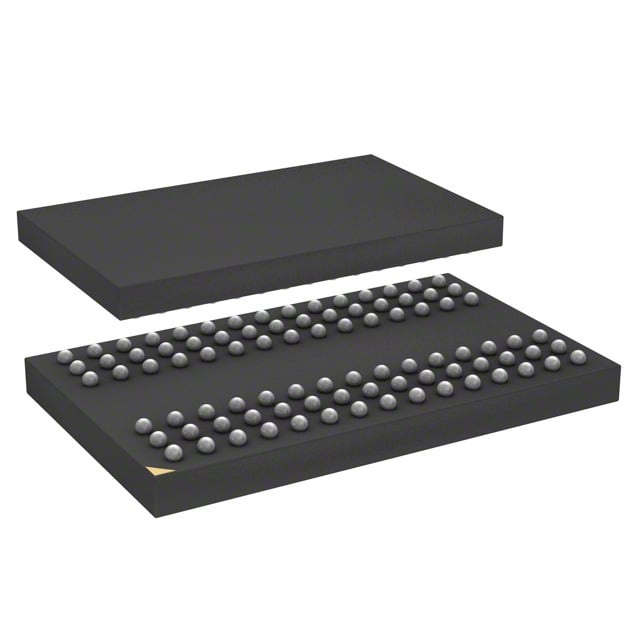
| Device Package | 90-TFBGA (8x13) | Memory Format | DRAM | Technology | SDRAM | ||
|---|---|---|---|---|---|---|---|
| Memory Size | 256 Mbit | Access Time | 5.4 ns | Grade | Industrial | ||
| Clock Frequency | 143 MHz | Voltage | 3V ~ 3.6V | Memory Type | Volatile | ||
| Operating Temperature | -40°C ~ 85°C (TA) | Write Cycle Time Word Page | N/A | Packaging | 90-TFBGA | ||
| Mounting Method | Volatile | Memory Interface | Parallel | Memory Organization | 8M x 32 | ||
| Moisture Sensitivity Level | 3 (168 Hours) | RoHS Compliance | ROHS3 Compliant | REACH Compliance | REACH Unaffected | ||
| Qualification | N/A | ECCN | EAR99 | HTS Code | 8542.32.0024 |
Overview of IS42S32800D-7BLI-TR – IC DRAM 256MBIT PAR 90TFBGA
The IS42S32800D-7BLI-TR is a 256 Mbit synchronous DRAM organized as 8M × 32 with a quad-bank architecture and fully synchronous interface. It implements pipeline architecture with all signals referenced to the rising edge of the clock to support burst transfers and predictable timing.
Designed for 3.3 V memory systems, this parallel-interface SDRAM targets applications that require deterministic, burst-capable volatile memory with support for programmable CAS latency, auto/self refresh and internal bank interleaving to help hide row precharge time.
Key Features
- Memory Core & Organization 256 Mbit SDRAM configured as 8M × 32 (2M × 32 × 4 banks) with internal bank architecture for improved row access efficiency.
- Performance & Timing Rated for a 143 MHz clock frequency with an access time of 5.4 ns (device -7 timing). Programmable CAS latency options and burst operation support enable flexible timing and throughput trade-offs.
- Burst and Sequencing Programmable burst lengths (1, 2, 4, 8, full page) and selectable burst sequences (sequential/interleave) allow optimized block transfers and memory throughput.
- Refresh & Power Modes Supports Auto Refresh and Self Refresh modes with 4096 refresh cycles per refresh interval options (documented 16 ms or 64 ms depending on grade), plus power-down capability to reduce standby power.
- Interface & Logic Levels Fully synchronous LVTTL-compatible interface with all signals registered on the rising clock edge for deterministic system timing.
- Power Supply Single-supply operation at 3.3 V ±0.3 V (listed as 3.0 V–3.6 V), simplifying integration into standard 3.3 V memory systems.
- Package & Temperature Supplied in a 90-ball TF-BGA (8×13) package; operating temperature range −40 °C to +85 °C as specified for the commercial/industrial grade.
Typical Applications
- System Memory Subsystems Provides burst-capable volatile storage for 3.3 V memory systems that require predictable synchronous timing and bank interleaving.
- Data Buffering Used as a high-throughput buffer for subsystems that need programmable burst lengths and rapid column access every clock cycle.
- Embedded Memory for 3.3 V Designs Suitable for embedded platforms requiring LVTTL-compatible synchronous DRAM with self-refresh and auto-refresh support.
Unique Advantages
- Deterministic Synchronous Operation: All signals referenced to the positive clock edge and LVTTL interface simplify timing closure and system design.
- Flexible Burst Control: Programmable burst length and sequence support reduce controller complexity for block transfers and streaming data patterns.
- Bank Interleaving: Internal multi-bank architecture hides row precharge delays, improving effective throughput for interleaved access patterns.
- Robust Refresh Options: Auto Refresh and Self Refresh modes with configurable refresh intervals enable reliable data retention and power-management trade-offs.
- Standard 3.3 V Supply: Compatibility with 3.3 V ±0.3 V systems simplifies integration into established memory power rails.
- Compact BGA Package: 90-TFBGA (8×13) package provides a high-density footprint suitable for space-constrained boards.
Why Choose IC DRAM 256MBIT PAR 90TFBGA?
The IS42S32800D-7BLI-TR combines a 256 Mbit synchronous DRAM core with programmable latency, burst control and internal bank architecture to deliver predictable, high-rate burst transfers for 3.3 V systems. Its LVTTL synchronous interface and self/auto-refresh capabilities make it appropriate for designs that require straightforward timing integration and reliable data retention.
This part is well suited to engineers building embedded systems or memory subsystems that need deterministic performance, flexible burst behavior and a compact BGA package. The combination of documented timing (143 MHz, 5.4 ns access), refresh modes and standard supply voltage supports scalability and stable operation across typical industrial temperature ranges.
Request a quote or contact sales to discuss availability, lead times and pricing for IS42S32800D-7BLI-TR.