IS42S32800D-7BL-TR
| Part Description |
IC DRAM 256MBIT PAR 90TFBGA |
|---|---|
| Quantity | 278 Available (as of June 8, 2026) |

| Product Category | Memory |
|---|---|
| Manufacturer | Integrated Silicon Solution Inc |
| Manufacturing Status | Obsolete |
| Manufacturer Standard Lead Time | Contact Us |
| Datasheet |
Specifications & Environmental
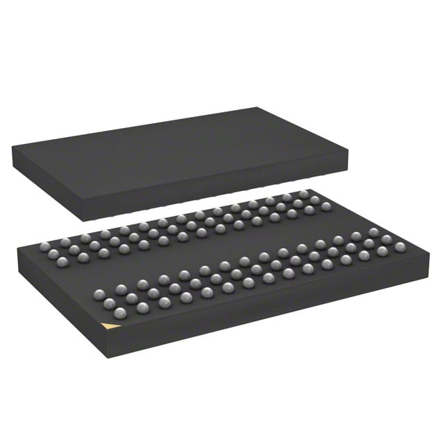
| Device Package | 90-TFBGA (8x13) | Memory Format | DRAM | Technology | SDRAM | ||
|---|---|---|---|---|---|---|---|
| Memory Size | 256 Mbit | Access Time | 5.4 ns | Grade | Commercial | ||
| Clock Frequency | 143 MHz | Voltage | 3V ~ 3.6V | Memory Type | Volatile | ||
| Operating Temperature | 0°C ~ 70°C (TA) | Write Cycle Time Word Page | N/A | Packaging | 90-TFBGA | ||
| Mounting Method | Volatile | Memory Interface | Parallel | Memory Organization | 8M x 32 | ||
| Moisture Sensitivity Level | 3 (168 Hours) | RoHS Compliance | ROHS3 Compliant | REACH Compliance | REACH Unaffected | ||
| Qualification | N/A | ECCN | EAR99 | HTS Code | 8542.32.0024 |
Overview of IS42S32800D-7BL-TR – IC DRAM 256MBIT PAR 90TFBGA
The IS42S32800D-7BL-TR is a 256Mbit synchronous DRAM organized as 8M × 32 (2M × 32 × 4 banks) in a 90-TFBGA (8×13) package. It is a fully synchronous, pipeline-architecture SDRAM designed for 3.3V memory systems and referenced to the rising edge of the clock.
Designed for systems that require high-speed, burst-capable parallel memory, this device provides programmable burst lengths and sequences, internal banking for hidden row access/precharge, and power-saving modes such as self-refresh and power-down.
Key Features
- Core Memory Architecture — 8M × 32 organization (2M × 32 × 4 banks) providing 256Mbit of volatile SDRAM storage with internal banking to hide row access and precharge.
- Performance — Supports a 143 MHz clock frequency (‑7 speed grade) with an access time from clock of 5.4 ns (CAS latency = 3).
- Programmable Burst and CAS — Programmable burst lengths (1, 2, 4, 8, full page) and burst sequences (sequential/interleave), with selectable CAS latency of 2 or 3 clocks.
- Refresh and Power Management — Auto Refresh and Self Refresh support; refresh options include 4096 cycles per 16 ms (A2 grade) or per 64 ms for commercial/A1 grades. Includes power-down capability.
- Interface and Signaling — LVTTL-compatible inputs and outputs with a parallel memory interface for synchronous burst read/write operations and random column address changes every clock cycle.
- Supply and Temperature — Single power supply: 3.3V (3.0V–3.6V tolerance) and commercial operating temperature range 0°C to +70°C.
- Package — 90-ball TF-BGA (8×13) supplier device package suitable for compact board-level integration.
Typical Applications
- Memory subsystems — Use as a 256Mbit synchronous DRAM component within 3.3V memory systems requiring pipelined, banked SDRAM architecture.
- Board-level embedded designs — Suitable for compact PCBs that accommodate a 90-TFBGA (8×13) package and operate in commercial temperature ranges (0°C–70°C).
- High-speed burst buffering — Appropriate where programmable burst lengths, interleave/sequential burst sequencing, and random column addressing per clock cycle are required for burst read/write operations.
- Low-power standby scenarios — Systems that leverage Self Refresh and power-down modes to reduce activity during idle periods.
Unique Advantages
- Quad-bank architecture: Internal 4-bank organization enables bank interleaving to hide precharge time and maintain continuous data flow during burst operations.
- Flexible burst control: Programmable burst lengths and sequences allow designers to match memory transfers to system data patterns and throughput requirements.
- Deterministic timing: Fully synchronous operation with LVTTL signaling and defined CAS latency options provides predictable timing for system integration.
- Standard 3.3V supply range: Operates with a single 3.3V supply (3.0V–3.6V), simplifying power-rail design for legacy and common memory systems.
- Compact BGA footprint: 90-TFBGA (8×13) packaging reduces board area while supporting high pin density for parallel memory interfaces.
Why Choose IC DRAM 256MBIT PAR 90TFBGA?
The IS42S32800D-7BL-TR provides a verified 256Mbit SDRAM solution with synchronous, banked architecture and programmable burst capabilities tailored for systems that require predictable, high-speed parallel memory. With a 143 MHz clock rating for the -7 speed grade, selectable CAS latency, and LVTTL-compatible interfacing, this device is suited to designs that need controlled timing and flexible burst behavior.
This part is appropriate for engineers specifying compact BGA-mounted SDRAM for commercial-temperature applications running from a standard 3.3V supply, offering self-refresh and auto-refresh options for power and retention strategies.
Request a quote or submit an inquiry to obtain pricing, availability, and lead-time information for IS42S32800D-7BL-TR.