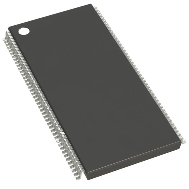
IS42S32800D-7TL
| Part Description |
IC DRAM 256MBIT PAR 86TSOP II |
|---|---|
| Quantity | 203 Available (as of June 15, 2026) |
| Product Category | Memory |
|---|---|
| Manufacturer | Integrated Silicon Solution Inc |
| Manufacturing Status | Active |
| Manufacturer Standard Lead Time | 12 Weeks |
| Datasheet |
Specifications & Environmental
| Device Package | 86-TSOP II | Memory Format | DRAM | Technology | SDRAM | ||
|---|---|---|---|---|---|---|---|
| Memory Size | 256 Mbit | Access Time | 5.4 ns | Grade | Commercial | ||
| Clock Frequency | 143 MHz | Voltage | 3V ~ 3.6V | Memory Type | Volatile | ||
| Operating Temperature | 0°C ~ 70°C (TA) | Write Cycle Time Word Page | N/A | Packaging | 86-TFSOP (0.400", 10.16mm Width) | ||
| Mounting Method | Volatile | Memory Interface | Parallel | Memory Organization | 8M x 32 | ||
| Moisture Sensitivity Level | 3 (168 Hours) | RoHS Compliance | ROHS3 Compliant | REACH Compliance | REACH Unaffected | ||
| Qualification | N/A | ECCN | EAR99 | HTS Code | 8542.32.0024 |
Overview of IS42S32800D-7TL – IC DRAM 256MBIT PAR 86TSOP II
The IS42S32800D-7TL is a 256Mbit synchronous DRAM device organized as 8M × 32 with an internal quad-bank architecture (2M × 32 × 4 banks). It implements a fully synchronous pipeline architecture with all signals referenced to the rising edge of the clock, providing predictable timing for parallel memory systems.
This device targets 3.3V memory systems and delivers programmable burst operation, selectable CAS latency, and built-in refresh modes for reliable dynamic memory operation in commercial-temperature designs.
Key Features
- Memory Architecture and Capacity 256 Mbit SDRAM organized as 8M × 32 with four internal banks (2M × 32 × 4), suitable for parallel memory subsystems requiring 32-bit data width.
- Performance Supports a clock frequency of 143 MHz (‑7 timing) with an access time from clock of 5.4 ns (CAS latency = 3). Programmable CAS latency options (2 or 3 clocks) allow timing flexibility.
- Synchronous Interface Fully synchronous operation with all inputs and outputs registered on the positive clock edge and LVTTL-compatible signaling for predictable system timing.
- Burst and Sequencing Programmable burst lengths (1, 2, 4, 8, full page) and selectable burst sequence (sequential or interleave). Supports burst read/write and burst read/single write operations with burst termination options.
- Power and Refresh Single power supply: 3.3V ±0.3V (3.0–3.6V supply range). Supports Auto Refresh (CBR) and Self Refresh; refresh counts documented as 4,096 cycles per 16 ms (A2 grade) or 64 ms (Commercial/Industrial/A1 grades).
- Package and Temperature Supplied in an 86‑pin TSOP‑II (0.400", 10.16 mm width) package. The specified operating temperature range for this commercial-grade device is 0°C to +70°C; datasheet lists additional package and temperature grade options.
Typical Applications
- Synchronous memory subsystems Provides 256 Mbit of parallel SDRAM for systems designed around 3.3V synchronous memory interfaces.
- Board-level DRAM expansion Acts as a 32-bit wide DRAM component for designers needing quad-bank, burst-capable memory with programmable CAS latency.
- Systems requiring structured refresh control Useful where Auto Refresh and Self Refresh modes with documented refresh counts are required for memory integrity.
Unique Advantages
- Quad-bank organization: Internal 4-bank architecture enables interleaving between banks to hide row precharge and improve sustained throughput.
- Flexible timing options: Programmable CAS latency (2 or 3 clocks) and multiple burst lengths/sequences allow tailoring performance to system timing constraints.
- Comprehensive refresh modes: Auto Refresh and Self Refresh support with documented refresh cycle counts for different grades simplifies system power/retention strategies.
- Synchronous LVTTL interface: Registered inputs/outputs on the clock edge provide deterministic timing for parallel SDRAM designs.
- Standard TSOP-II packaging: 86‑pin TSOP‑II form factor (0.400", 10.16 mm width) for common board-level mounting and footprint compatibility.
Why Choose IS42S32800D-7TL?
The IS42S32800D-7TL combines a 256 Mbit quad-bank SDRAM architecture with programmable burst control and selectable CAS latency to offer designers predictable, synchronous memory behavior in 3.3V systems. Its LVTTL interface and registered clocked I/O simplify timing closure for parallel memory subsystems, while Auto Refresh and Self Refresh modes support reliable data retention strategies.
This commercial-grade TSOP-II packaged device is well suited to board-level memory expansion and system designs that require a documented timing and refresh feature set at a 143 MHz clock frequency (‑7 timing). The datasheet provides additional packaging and temperature grade options for designs that may require different environmental ranges or package formats.
Request a quote or contact sales to discuss availability, lead times, and integration details for IS42S32800D-7TL.