IS42S32800G-6BI
| Part Description |
IC DRAM 256MBIT PAR 90TFBGA |
|---|---|
| Quantity | 1,146 Available (as of June 17, 2026) |

| Product Category | DRAM Memory |
|---|---|
| Manufacturer | Integrated Silicon Solution Inc |
| Manufacturing Status | Obsolete |
| Manufacturer Standard Lead Time | Contact Us |
| Datasheet |
Specifications & Environmental
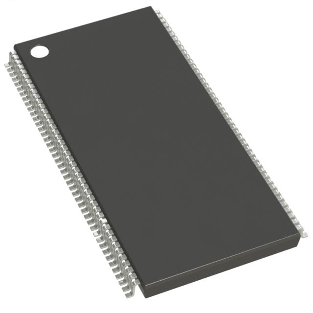
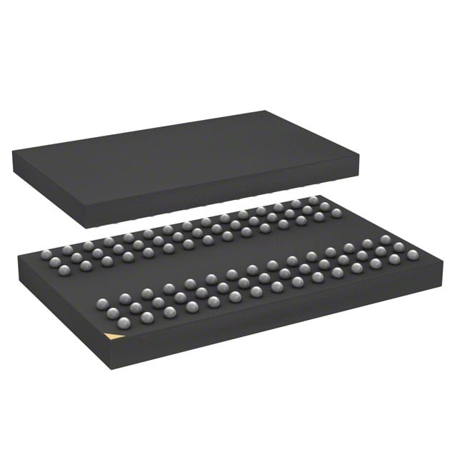
| Device Package | 90-TFBGA (8x13) | Memory Format | DRAM | Technology | SDRAM | ||
|---|---|---|---|---|---|---|---|
| Memory Size | 256 Mbit | Access Time | 5.4 ns | Grade | Industrial | ||
| Clock Frequency | 166 MHz | Voltage | 3V ~ 3.6V | Memory Type | Volatile | ||
| Operating Temperature | -40°C ~ 85°C (TA) | Write Cycle Time Word Page | N/A | Packaging | 90-TFBGA | ||
| Mounting Method | Volatile | Memory Interface | Parallel | Memory Organization | 8M x 32 | ||
| Moisture Sensitivity Level | 3 (168 Hours) | RoHS Compliance | ROHS Compliant | REACH Compliance | REACH Unaffected | ||
| Qualification | N/A | ECCN | EAR99 | HTS Code | 8542.32.0024 |
Overview of IS42S32800G-6BI – 256Mbit Synchronous DRAM, 90-TFBGA
The IS42S32800G-6BI is a 256 Mbit synchronous DRAM organized as 8M × 32 with a parallel memory interface. It implements a quad-bank, fully synchronous pipeline architecture with all signals referenced to the rising edge of the clock, and operates from a single 3.3 V supply.
This device is intended for systems that require a 256 Mbit parallel SDRAM for temporary data storage and buffering, offering programmable burst lengths, selectable CAS latency, and self-refresh/auto-refresh capabilities for managed data retention and throughput.
Key Features
- Core / Architecture Quad-bank synchronous DRAM organized as 8M × 32 (2M × 32 × 4 banks) with pipeline architecture; all inputs/outputs referenced to the rising clock edge.
- Memory Capacity & Organization 256 Mbit total capacity arranged as 8M × 32 providing wide 32-bit data paths for parallel memory systems.
- Performance Supports clock frequencies including 166 MHz (device -6 grade) with an access time from clock of approximately 5.4 ns and programmable CAS latency of 2 or 3 clocks.
- Burst & Access Modes Programmable burst length (1, 2, 4, 8, full page) and selectable burst sequence (sequential or interleave); supports burst read/write and read/single write operations with burst termination commands.
- Refresh & Low-Power Modes Auto Refresh (CBR) and Self Refresh supported; refresh cycle count documented (4096 cycles with timing dependent on grade).
- Power Single power supply range listed as 3.0 V to 3.6 V (typical operation at 3.3 V ±0.3 V).
- Interface & Logic LVTTL-compatible interface signals and random column address capability every clock cycle.
- Package & Temperature 90-ball TF-BGA package (90-TFBGA, 8×13 ball array) with an operating ambient temperature range of −40 °C to +85 °C (TA) for the specified product listing.
Typical Applications
- Embedded Memory Subsystems Provides 256 Mbit parallel SDRAM capacity for temporary data storage and buffering in embedded systems that require synchronous DRAM.
- High-Speed Buffering Used where pipeline architecture and programmable burst operations are needed for bursty data traffic and temporary buffering.
- Memory Interface Modules Suitable for designs that require a 32-bit-wide parallel SDRAM device with selectable CAS latency and burst sequencing.
Unique Advantages
- Pipeline Synchronous Design: Enables predictable timing by referencing all signals to the rising clock edge, simplifying timing closure for synchronous systems.
- Flexible Burst Control: Programmable burst lengths and sequence modes provide flexibility to match system data access patterns and maximize effective throughput.
- Selectable CAS Latency: CAS latency options (2 or 3 clocks) let designers trade between latency and clock rate based on system timing requirements.
- Single 3.3 V Supply: Operates from a single 3.0 V to 3.6 V supply (typical 3.3 V), simplifying power rail design for legacy 3.3 V memory systems.
- Compact BGA Packaging: 90-TFBGA (8×13) footprint minimizes board area while providing a 32-bit data interface in a ball-grid array package.
- Temperature Range: Rated for −40 °C to +85 °C (TA) in the listed product configuration for designs requiring extended ambient operation.
Why Choose IS42S32800G-6BI?
IS42S32800G-6BI combines a 256 Mbit capacity with a fully synchronous, quad-bank pipeline architecture and flexible burst/CAS programmability to address parallel SDRAM requirements in systems needing deterministic timing and managed refresh behavior. Its single 3.3 V supply, LVTTL interface, and compact 90-TFBGA package make it appropriate for designs constrained by board space and legacy 3.3 V memory interfaces.
This device is suitable for engineers specifying a 256 Mbit parallel SDRAM with documented timing (e.g., 166 MHz operation and 5.4 ns access-from-clock for the -6 grade) and the functional features necessary for buffered data storage and burst transfer control.
Request a quote or submit an inquiry to start sourcing IS42S32800G-6BI for your design and procurement evaluation.