IS42S32800D-7TLI
| Part Description |
IC DRAM 256MBIT PAR 86TSOP II |
|---|---|
| Quantity | 366 Available (as of June 14, 2026) |

| Product Category | Memory |
|---|---|
| Manufacturer | Integrated Silicon Solution Inc |
| Manufacturing Status | Obsolete |
| Manufacturer Standard Lead Time | Contact Us |
| Datasheet |
Specifications & Environmental
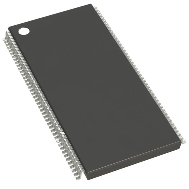
| Device Package | 86-TSOP II | Memory Format | DRAM | Technology | SDRAM | ||
|---|---|---|---|---|---|---|---|
| Memory Size | 256 Mbit | Access Time | 5.4 ns | Grade | Industrial | ||
| Clock Frequency | 143 MHz | Voltage | 3V ~ 3.6V | Memory Type | Volatile | ||
| Operating Temperature | -40°C ~ 85°C (TA) | Write Cycle Time Word Page | N/A | Packaging | 86-TFSOP (0.400", 10.16mm Width) | ||
| Mounting Method | Volatile | Memory Interface | Parallel | Memory Organization | 8M x 32 | ||
| Moisture Sensitivity Level | 3 (168 Hours) | RoHS Compliance | ROHS3 Compliant | REACH Compliance | REACH Unaffected | ||
| Qualification | N/A | ECCN | EAR99 | HTS Code | 8542.32.0024 |
Overview of IS42S32800D-7TLI – IC DRAM 256MBIT PAR 86TSOP II
The IS42S32800D-7TLI is a 256Mbit synchronous DRAM (SDRAM) organized as 8M × 32 with an internal quad-bank architecture and a parallel memory interface. It is a high-speed, fully synchronous DRAM device designed for 3.3V systems and referenced to the rising edge of the clock.
Targeted at systems that require deterministic, burst-capable parallel memory, this device provides programmable burst lengths and CAS latency options, making it suitable for commercial and industrial environments where 3.3V supply operation and operation from -40°C to +85°C are required.
Key Features
- Core / Architecture 8M × 32 organization (2M × 32 × 4 banks) with internal bank structure to hide row access and precharge delays.
- Memory Capacity 256 Mbit DRAM in a parallel memory format.
- Clock & Timing Supports a clock frequency of 143 MHz (‑7 speed grade); programmable CAS latency (2 or 3 clocks) with an access time of 5.4 ns at CAS latency = 3.
- Burst and Sequencing Programmable burst lengths (1, 2, 4, 8, full page) and selectable burst sequence (sequential/interleave); supports burst read/write and burst read/single write operations with burst termination.
- Refresh & Power Management Auto Refresh and Self Refresh modes; refresh rate examples include 4096 cycles per 16 ms (A2 grade) or 64 ms (Commercial/Industrial/A1 grade).
- Interface & Logic Levels LVTTL compatible I/O; fully synchronous interface with all inputs and outputs referenced to the positive clock edge.
- Supply Voltage Single power supply operation at 3.3V ±0.3V (3.0V to 3.6V).
- Package & Temperature Range 86-pin TSOP-II (86-TFSOP, 0.400", 10.16 mm width) package; operating temperature range −40°C to +85°C (TA).
Typical Applications
- Embedded Systems High-speed parallel SDRAM for 3.3V memory subsystems in embedded designs requiring deterministic burst access.
- Industrial Electronics Memory solutions for industrial equipment that must operate across −40°C to +85°C.
- Networking & Communications Buffer and packet memory applications that benefit from quad-bank architecture and fast burst transfers.
- High-Throughput Data Paths Applications requiring wide data paths (32-bit) and programmable burst sequencing for sustained data movement.
Unique Advantages
- High-throughput parallel interface: 32-bit data width combined with up to 143 MHz clocking (‑7) enables substantial parallel data bandwidth.
- Flexible latency and burst control: Programmable CAS latency (2 or 3) and multiple burst length/sequence options let designers tune performance to application needs.
- Banked architecture for reduced cycle overhead: Quad-bank internal organization permits interleaving between banks to hide precharge time and improve effective throughput.
- Power and refresh management: Auto Refresh and Self Refresh modes simplify refresh handling and support system power-saving strategies.
- Industrial temperature support: Specified operation from −40°C to +85°C (TA) for use in temperature-challenging deployments.
- Standard TSOP-II footprint: 86-pin TSOP-II package (10.16 mm width) for compatibility with established board designs.
Why Choose IS42S32800D-7TLI?
The IS42S32800D-7TLI from Integrated Silicon Solution, Inc. offers a practical combination of capacity, predictable latency, and burst flexibility in a 3.3V synchronous DRAM. Its quad-bank organization, LVTTL synchronous interface, and programmable burst/CAS options make it well suited to designs that need parallel, high-throughput memory in commercial and industrial temperature ranges.
Engineers specifying this device benefit from clear timing options (including a 143 MHz speed grade and 5.4 ns access at CL=3), standard TSOP-II packaging, and integrated refresh/power features that reduce memory management complexity and help maintain robust long-term operation.
Request a quote or submit a procurement inquiry for the IS42S32800D-7TLI to receive pricing and lead-time information for your project.