IS42S83200G-7BL
| Part Description |
IC DRAM 256MBIT PAR 54TFBGA |
|---|---|
| Quantity | 98 Available (as of June 14, 2026) |

| Product Category | Memory |
|---|---|
| Manufacturer | Integrated Silicon Solution Inc |
| Manufacturing Status | Obsolete |
| Manufacturer Standard Lead Time | Contact Us |
| Datasheet |
Specifications & Environmental
| Device Package | 54-TFBGA (8x8) | Memory Format | DRAM | Technology | SDRAM | ||
|---|---|---|---|---|---|---|---|
| Memory Size | 256 Mbit | Access Time | 5.4 ns | Grade | Commercial | ||
| Clock Frequency | 143 MHz | Voltage | 3V ~ 3.6V | Memory Type | Volatile | ||
| Operating Temperature | 0°C ~ 70°C (TA) | Write Cycle Time Word Page | N/A | Packaging | 54-TFBGA | ||
| Mounting Method | Volatile | Memory Interface | Parallel | Memory Organization | 32M x 8 | ||
| Moisture Sensitivity Level | 3 (168 Hours) | RoHS Compliance | ROHS3 Compliant | REACH Compliance | REACH Unaffected | ||
| Qualification | N/A | ECCN | EAR99 | HTS Code | 8542.32.0024 |
Overview of IS42S83200G-7BL – IC DRAM 256MBIT PAR 54TFBGA
The IS42S83200G-7BL is a 256 Mbit synchronous DRAM organized as 32M × 8 with internal bank architecture and pipeline operation for high-speed data transfer. It implements a fully synchronous, parallel SDRAM interface with programmable burst and CAS options to support a range of read/write access patterns.
Designed for systems that require parallel SDRAM memory with compact BGA packaging and standard 3.3 V single-supply operation, the device provides selectable refresh modes and self-refresh for system-level memory management and power sequencing.
Key Features
- Core / Architecture Fully synchronous SDRAM with internal bank architecture and pipeline operation; all I/O referenced to the rising edge of the clock.
- Memory Organization 256 Mbit capacity arranged as 32M × 8 with 4 internal banks.
- Performance Speed grade -7 supports up to 143 MHz clock frequency with 5.4 ns access time (from clock) and programmable CAS latency (2 or 3 clocks).
- Burst and Sequencing Programmable burst lengths (1, 2, 4, 8, full page) and selectable burst sequence (sequential/interleave); supports burst read/write and burst read/single write operations with burst termination options.
- Refresh and Low-Power Modes Auto Refresh (CBR) and Self Refresh supported; 8K refresh cycles per refresh interval (commercial/industrial A1: 64 ms; A2: 32 ms documented in datasheet).
- Interface LVTTL-compatible signals with random column address capability every clock cycle for predictable data throughput.
- Power Single power supply: 3.3 V ±0.3 V (3.0 V to 3.6 V operational range).
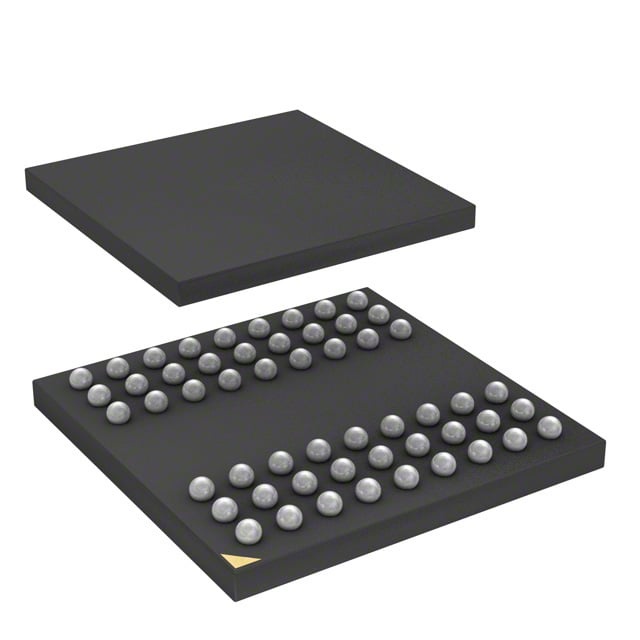
- Package and Mounting 54-ball TFBGA (8 × 8) package for compact board-level integration; supplier device package listed as 54-TFBGA (8×8).
- Operating Temperature Commercial grade operating range 0°C to +70°C (TA).
Typical Applications
- Parallel memory subsystems Use where a 256 Mbit synchronous parallel DRAM is required for high-throughput buffering and temporary storage.
- Embedded systems Suitable for embedded designs that require synchronous DRAM with selectable burst behavior and self-refresh capability.
- Board-level memory expansion Compact 54-TFBGA package enables dense board layouts that need a 3.3 V single-supply SDRAM solution.
Unique Advantages
- High-speed synchronous operation: Pipeline architecture with a 143 MHz clock option and 5.4 ns access time from clock delivers deterministic timing for synchronous designs.
- Flexible data access: Programmable burst lengths and selectable sequential/interleave burst sequences allow tailored memory access patterns to match system needs.
- Standard single-supply power: Operates from a 3.3 V single supply (3.0 V to 3.6 V), simplifying power-rail design.
- Refresh and retention modes: Auto Refresh and Self Refresh support reduce system refresh management overhead and help with low-power retention.
- Compact BGA packaging: 54-ball TFBGA (8×8) package provides a small footprint for dense board integration.
- Predictable timing controls: Programmable CAS latency (2 or 3) and LVTTL signaling give designers control over timing and interface compatibility.
Why Choose IS42S83200G-7BL?
The IS42S83200G-7BL offers a combination of synchronous, high-throughput SDRAM architecture and flexible access features suitable for designs requiring compact, parallel memory. Its 32M × 8 organization, programmable burst behavior, and supported refresh modes provide designers with deterministic timing and memory management options for a variety of system-level buffering and temporary storage needs.
With a standard 3.3 V supply, LVTTL signaling, and a 54-TFBGA package, this device is positioned for board-level memory expansion where size, synchronous operation, and selectable timing parameters are important. The documented operating range and refresh options support integration into commercial-grade designs.
Request a quote or submit an inquiry to receive pricing and availability for IS42S83200G-7BL and to discuss part integration and delivery options.