IS42S83200G-7BLI
| Part Description |
IC DRAM 256MBIT PAR 54TFBGA |
|---|---|
| Quantity | 1,072 Available (as of June 15, 2026) |
| Product Category | DRAM Memory |
|---|---|
| Manufacturer | Integrated Silicon Solution Inc |
| Manufacturing Status | Obsolete |
| Manufacturer Standard Lead Time | Contact Us |
| Datasheet |
Specifications & Environmental
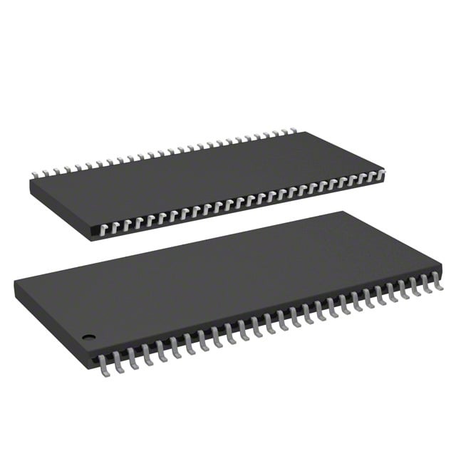
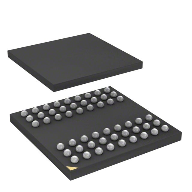
| Device Package | 54-TFBGA (8x8) | Memory Format | DRAM | Technology | SDRAM | ||
|---|---|---|---|---|---|---|---|
| Memory Size | 256 Mbit | Access Time | 5.4 ns | Grade | Industrial | ||
| Clock Frequency | 143 MHz | Voltage | 3V ~ 3.6V | Memory Type | Volatile | ||
| Operating Temperature | -40°C ~ 85°C (TA) | Write Cycle Time Word Page | N/A | Packaging | 54-TFBGA | ||
| Mounting Method | Volatile | Memory Interface | Parallel | Memory Organization | 32M x 8 | ||
| Moisture Sensitivity Level | 3 (168 Hours) | RoHS Compliance | ROHS3 Compliant | REACH Compliance | REACH Unaffected | ||
| Qualification | N/A | ECCN | EAR99 | HTS Code | 8542.32.0024 |
Overview of IS42S83200G-7BLI – IC DRAM 256MBIT PAR 54TFBGA
The IS42S83200G-7BLI is a 256 Mbit synchronous DRAM (SDRAM) organized as 32M × 8 with four internal banks and a pipeline architecture for high-speed data transfer. It provides a parallel SDRAM interface with programmable burst modes and timing options for use in systems requiring synchronized, high-throughput memory access.
Key attributes include a 143 MHz clock frequency rating (‑7 speed grade), programmable CAS latency, and support for auto- and self-refresh modes, making it suitable for embedded and system memory buffering applications that demand predictable synchronous operation.
Key Features
- Memory Core & Organization 256 Mbit SDRAM organized as 32M × 8 with four internal banks to support efficient row/column operations and bank interleaving.
- Synchronous Pipeline Architecture Fully synchronous design with all signals referenced to the rising edge of the clock to enable deterministic timing and pipeline data transfer.
- Speed Grades & Timing Clock frequency up to 143 MHz for the -7 grade with access times as low as 5.4 ns and programmable CAS latency (2 or 3 clocks).
- Burst Control Programmable burst length (1, 2, 4, 8, full page) and selectable burst sequence (sequential or interleave) for flexible read/write transfer patterns.
- Refresh & Retention Supports auto refresh (CBR) and self refresh; refresh count options include 8K cycles every 32 ms (A2 grade) or 64 ms (commercial/industrial/A1 grade).
- Interface & Logic Levels LVTTL-compatible interface with parallel memory access signals for integration with standard SDRAM controllers.
- Power Single power supply: 3.3 V ± 0.3 V (specified supply range 3.0 V to 3.6 V).
- Package & Temperature Supplied in a 54-ball TFBGA (8 × 8) package with an operating ambient temperature range of -40°C to +85°C.
Typical Applications
- High-speed buffering Used where pipeline SDRAM buffering is required to support sustained parallel data transfers and burst operations.
- System memory expansion Suitable for designs needing a 256 Mbit parallel SDRAM device with configurable burst and timing behavior for controller-managed memory.
- Embedded controllers and FPGA memory Employed as external synchronous memory for embedded systems or FPGA-based platforms that utilize parallel SDRAM interfaces.
Unique Advantages
- Deterministic synchronous operation: Fully synchronous inputs and outputs referenced to the clock simplify timing analysis and controller integration.
- Flexible performance tuning: Programmable CAS latency (2 or 3) and multiple burst lengths/sequences let designers optimize latency and throughput for application needs.
- Robust refresh options: Auto and self-refresh support plus selectable refresh rates (8K cycles/32 ms or 64 ms) provide adaptability across grades and power profiles.
- Industry-standard voltage: Operates from 3.0 V to 3.6 V (nominal 3.3 V), matching common system power rails.
- Compact BGA package: 54-ball TFBGA (8×8) offers a small-footprint surface-mount solution for space-constrained PCB designs.
- Wide operating temperature: Specified for -40°C to +85°C ambient operation for use in temperature-variable environments.
Why Choose IS42S83200G-7BLI?
The IS42S83200G-7BLI delivers a balanced combination of synchronous pipeline architecture, flexible burst control, and selectable timing that suits designs requiring predictable parallel SDRAM performance. Its 32M × 8 organization, programmable CAS latencies, and refresh modes allow system architects to tune memory behavior to specific throughput and power trade-offs.
This device is appropriate for engineers implementing external SDRAM in embedded systems, controllers, or FPGA platforms who need compact packaging, standard 3.3 V operation, and an industrial temperature range. The IS42S83200G-7BLI provides verifiable, datasheet-defined characteristics for reliable integration into long-term designs.
Request a quote or submit an inquiry to receive pricing and availability information for the IS42S83200G-7BLI.