IS42S83200G-7TL-TR
| Part Description |
IC DRAM 256MBIT PAR 54TSOP II |
|---|---|
| Quantity | 992 Available (as of June 15, 2026) |

| Product Category | Memory |
|---|---|
| Manufacturer | Integrated Silicon Solution Inc |
| Manufacturing Status | Obsolete |
| Manufacturer Standard Lead Time | Contact Us |
| Datasheet |
Specifications & Environmental
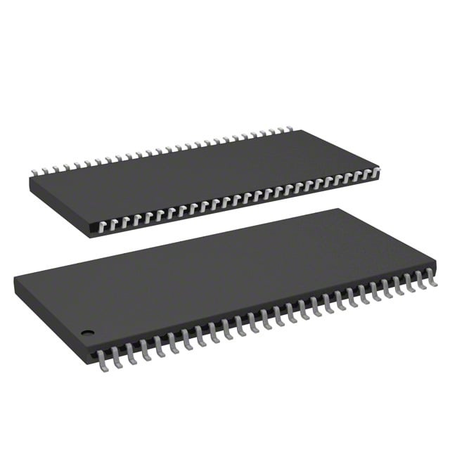
| Device Package | 54-TSOP II | Memory Format | DRAM | Technology | SDRAM | ||
|---|---|---|---|---|---|---|---|
| Memory Size | 256 Mbit | Access Time | 5.4 ns | Grade | Commercial | ||
| Clock Frequency | 143 MHz | Voltage | 3V ~ 3.6V | Memory Type | Volatile | ||
| Operating Temperature | 0°C ~ 70°C (TA) | Write Cycle Time Word Page | N/A | Packaging | 54-TSOP (0.400", 10.16mm Width) | ||
| Mounting Method | Volatile | Memory Interface | Parallel | Memory Organization | 32M x 8 | ||
| Moisture Sensitivity Level | 3 (168 Hours) | RoHS Compliance | ROHS3 Compliant | REACH Compliance | REACH Unaffected | ||
| Qualification | N/A | ECCN | EAR99 | HTS Code | 8542.32.0024 |
Overview of IS42S83200G-7TL-TR – IC DRAM 256MBIT PAR 54TSOP II
The IS42S83200G-7TL-TR is a 256 Mbit synchronous DRAM organized as 32M × 8 with four internal banks and a parallel memory interface. It uses a pipelined, fully synchronous architecture with all signals referenced to the rising edge of the clock to support high-speed data transfer.
Designed for systems requiring parallel SDRAM, this commercial-temperature (0°C to 70°C) device offers programmable burst control, selectable CAS latency, and standard 54-pin TSOP-II packaging to simplify integration into memory subsystems.
Key Features
- Memory Organization 256 Mbit SDRAM organized as 32M × 8 with four internal banks to support efficient row/column accesses and concurrent bank management.
- High‑Speed Synchronous Operation Fully synchronous SDRAM with a –7 speed grade rated for 143 MHz clock frequency and access time of 5.4 ns.
- Programmable Burst and Latency Supports programmable burst lengths (1, 2, 4, 8, full page), burst sequence (Sequential/Interleave), and CAS latency selectable between 2 and 3 clocks.
- Power Single power supply: 3.3 V ±0.3 V (3.0 V to 3.6 V supply range), suitable for standard 3.3 V memory systems.
- Interface LVTTL-compatible control interface with parallel SDRAM signaling referenced to the positive clock edge for predictable timing.
- Refresh and Self‑Refresh Supports Auto Refresh and Self Refresh modes; datasheet options include 8K refresh cycles every 32 ms (A2 grade) or 64 ms (commercial/A1/industrial grades).
- Package and Mounting 54-pin TSOP-II package (0.400", 10.16 mm width) optimized for PCB-level memory implementations.
- Commercial Temperature Range Rated for ambient operation from 0°C to +70°C (TA).
Typical Applications
- Embedded Systems Used as parallel SDRAM for system memory and high-speed data buffering where synchronous access and burst transfers are required.
- Data Buffering Suitable for applications that need predictable, pipelined memory transfers and burst read/write operations for transient data storage.
- Display/Frame Buffering Applicable where parallel SDRAM is required to support sequential or interleaved burst reads for frame and pixel data handling.
- Networking and Communications Can be deployed for packet buffering and transient storage in systems that use parallel synchronous memory interfaces.
Unique Advantages
- Fully Synchronous Pipeline Architecture: All signals referenced to the rising clock edge enable deterministic timing and simplified system timing design.
- Flexible Burst Control: Programmable burst length and sequence allow designers to optimize throughput for sequential or interleaved access patterns.
- Selectable CAS Latency: CAS latency choices (2 or 3 clocks) provide trade-offs between latency and maximum clock frequency for system tuning.
- Standard 3.3 V Supply: Operates on a single 3.3 V ±0.3 V supply to align with common memory power rails and simplify power design.
- Compact TSOP-II Footprint: 54-pin TSOP-II package supports high-density board layouts while maintaining standard pinout for SDRAM designs.
- Refresh Modes: Auto and Self Refresh support extended data retention strategies and low‑activity power management per the device grade.
Why Choose IS42S83200G-7TL-TR?
The IS42S83200G-7TL-TR provides a dependable 256 Mbit synchronous DRAM option with a pipelined, banked architecture and programmable timing features to match a range of parallel memory system requirements. Its –7 speed grade (143 MHz) and 5.4 ns access timing deliver predictable performance for designs that require synchronous burst transfers and low-latency access.
This device is well suited for engineers and procurement teams specifying commercial-temperature SDRAM in a 54-pin TSOP-II package who need standard 3.3 V operation, flexible burst and latency control, and support for Auto/Self Refresh modes as documented by the manufacturer.
Request a quote or submit an inquiry to check availability, pricing, and lead times for the IS42S83200G-7TL-TR.