IS42S83200G-7TLI-TR
| Part Description |
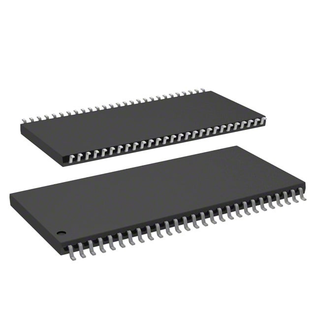
IC DRAM 256MBIT PAR 54TSOP II |
|---|---|
| Quantity | 535 Available (as of June 14, 2026) |

| Product Category | Memory |
|---|---|
| Manufacturer | Integrated Silicon Solution Inc |
| Manufacturing Status | Obsolete |
| Manufacturer Standard Lead Time | Contact Us |
| Datasheet |
Specifications & Environmental
| Device Package | 54-TSOP II | Memory Format | DRAM | Technology | SDRAM | ||
|---|---|---|---|---|---|---|---|
| Memory Size | 256 Mbit | Access Time | 5.4 ns | Grade | Industrial | ||
| Clock Frequency | 143 MHz | Voltage | 3V ~ 3.6V | Memory Type | Volatile | ||
| Operating Temperature | -40°C ~ 85°C (TA) | Write Cycle Time Word Page | N/A | Packaging | 54-TSOP (0.400", 10.16mm Width) | ||
| Mounting Method | Volatile | Memory Interface | Parallel | Memory Organization | 32M x 8 | ||
| Moisture Sensitivity Level | 3 (168 Hours) | RoHS Compliance | ROHS Compliant | REACH Compliance | REACH Unaffected | ||
| Qualification | N/A | ECCN | EAR99 | HTS Code | 8542.32.0024 |
Overview of IS42S83200G-7TLI-TR – IC DRAM 256Mbit PAR 54TSOP II
The IS42S83200G-7TLI-TR is a 256Mbit synchronous DRAM organized as 32M × 8 with internal bank architecture and pipeline operation. It provides fully synchronous, clock-referenced memory operation optimized for high-speed data transfer with a parallel LVTTL interface.
This device targets designs that require compact, clocked DRAM storage with programmable burst and timing features, delivered in a 54-pin TSOP-II package and specified for operation from -40°C to +85°C.
Key Features
- Memory Architecture 256Mbit SDRAM organized as 32M × 8 with multiple internal banks to hide row access/precharge and support pipelined operation.
- Clocked Performance -7 speed grade provides a clock frequency up to 143 MHz and an access time from clock of 5.4 ns (CAS latency = 3).
- Programmable Burst & Timing Programmable burst lengths (1, 2, 4, 8, full page) and burst sequence (sequential/interleave); programmable CAS latency (2 or 3 clocks).
- Refresh & Power Management Auto refresh and self-refresh supported; 8K refresh cycles with 32 ms (A2) or 64 ms (commercial/industrial/A1) refresh intervals as specified.
- Interface & Signaling Parallel memory interface with LVTTL signaling; all inputs and outputs referenced to the rising edge of the clock.
- Supply & Voltage Range Single-supply operation centered at 3.3 V (3.0 V to 3.6 V documented / 3.3 V ±0.3 V in datasheet).
- Package & Mounting 54-pin TSOP-II (0.400", 10.16 mm width) package for board-level mounting and compact system integration.
- Temperature Range Specified operating ambient temperature from -40°C to +85°C.
Typical Applications
- High-speed memory subsystems Use as synchronous DRAM storage in designs that require pipelined, clocked memory operation and predictable timing.
- Buffered data transfer Suitable for applications requiring burst reads/writes and programmable burst sequencing to support sustained data throughput.
- Temperature-conditioned designs Applicable where operation across -40°C to +85°C is required, leveraging the specified industrial temperature range.
Unique Advantages
- Synchronous pipeline architecture: Enables high-speed data transfer with all signals referenced to the clock rising edge for deterministic timing.
- Flexible timing and burst control: Programmable CAS latency and burst length/sequence allow tuning for system timing and throughput needs.
- Single-supply simplicity: Operates from a 3.3 V class supply (3.0–3.6 V range), simplifying power rail design.
- Compact TSOP-II footprint: 54-pin TSOP-II package provides a space-efficient option for board-level memory integration.
- Refresh and low-power modes: Auto-refresh and self-refresh support help maintain data integrity while managing refresh requirements.
- Deterministic LVTTL interface: Parallel LVTTL signaling and clock-referenced I/Os simplify timing closure in synchronous systems.
Why Choose IC DRAM 256MBIT PAR 54TSOP II?
The IS42S83200G-7TLI-TR combines a 256Mbit synchronous DRAM organization with pipeline architecture and programmable burst/timing features to deliver predictable, clocked memory performance in a compact 54-pin TSOP-II package. Its specified access timing (5.4 ns from clock at -7 grade) and 143 MHz clock capability (CAS latency = 3) make it suitable for designs that require deterministic, high-speed parallel memory.
This device is appropriate for engineers seeking a standardized synchronous DRAM building block with flexible timing, auto/self-refresh capabilities, and a documented operating range to -40°C. The combination of supply range, LVTTL interface, and package choice supports board-level integration in systems that rely on parallel SDRAM storage.
Request a quote or contact sales to discuss availability, lead times, and volume pricing for the IS42S83200G-7TLI-TR.