IS42S86400D-7TL
| Part Description |
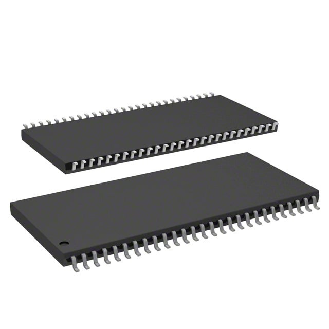
IC DRAM 512MBIT PAR 54TSOP II |
|---|---|
| Quantity | 363 Available (as of June 17, 2026) |

| Product Category | DRAM Memory |
|---|---|
| Manufacturer | Integrated Silicon Solution Inc |
| Manufacturing Status | Obsolete |
| Manufacturer Standard Lead Time | Contact Us |
| Datasheet |
Specifications & Environmental
| Device Package | 54-TSOP II | Memory Format | DRAM | Technology | SDRAM | ||
|---|---|---|---|---|---|---|---|
| Memory Size | 512 Mbit | Access Time | 5.4 ns | Grade | Commercial | ||
| Clock Frequency | 143 MHz | Voltage | 3V ~ 3.6V | Memory Type | Volatile | ||
| Operating Temperature | 0°C ~ 70°C (TA) | Write Cycle Time Word Page | N/A | Packaging | 54-TSOP (0.400", 10.16mm Width) | ||
| Mounting Method | Volatile | Memory Interface | Parallel | Memory Organization | 64M x 8 | ||
| Moisture Sensitivity Level | 3 (168 Hours) | RoHS Compliance | ROHS Compliant | REACH Compliance | REACH Unaffected | ||
| Qualification | N/A | ECCN | EAR99 | HTS Code | 8542.32.0028 |
Overview of IS42S86400D-7TL – IC DRAM 512Mbit Parallel, 54‑TSOP II
The IS42S86400D-7TL is a 512 Mbit synchronous DRAM organized as 64M × 8 with a parallel memory interface and pipeline architecture for high-speed data transfer. It implements fully synchronous operation with programmable burst control and internal bank management to support pipelined access patterns.
This device targets designs that require a commercial-temperature 512 Mbit SDRAM solution in a compact 54‑pin TSOP‑II package, operating from a 3.0 V to 3.6 V supply and offering selectable CAS latency and refresh modes for predictable timing behavior.
Key Features
- Memory Organization 64M × 8 organization providing 512 Mbit of volatile DRAM storage across four internal banks to support interleaved and pipelined accesses.
- Synchronous SDRAM Architecture Fully synchronous device with all signals referenced to the rising edge of the clock and pipeline architecture for high-speed transfers.
- Clock and Timing Rated for a clock frequency of 143 MHz (‑7 speed grade) with an access time from clock of 5.4 ns and programmable CAS latency options (2 or 3 clocks).
- Burst and Sequencing Programmable burst length (1, 2, 4, 8, full page) and selectable burst sequence (sequential or interleave) for flexible data streaming and throughput optimization.
- Refresh and Self‑Maintenance Supports Auto Refresh and Self Refresh with 8K refresh cycles every 64 ms to maintain data integrity.
- Interface and Signaling LVTTL-compatible interface with parallel memory bus and support for burst read/write and burst read/single write operations; burst termination via burst stop and precharge commands.
- Power Supply range specified as 3.0 V to 3.6 V for the device family, supporting typical 3.3 V system rails.
- Package and Temperature 54‑pin TSOP‑II package (0.400" / 10.16 mm width) and commercial operating temperature range of 0°C to +70°C.
Typical Applications
- High-speed memory subsystems Used where a parallel 512 Mbit SDRAM with programmable burst and low access time is required for pipelined data transfer.
- Buffering and temporary storage Provides volatile storage for system buffers that benefit from programmable burst lengths and sequential/interleaved access modes.
- Embedded system DRAM Fits compact board designs that require 512 Mbit density in a 54‑pin TSOP‑II package and commercial temperature operation.
Unique Advantages
- Flexible burst control: Programmable burst lengths (1, 2, 4, 8, full page) and selectable burst sequences allow tuning of throughput and latency for specific access patterns.
- Synchronous pipelined operation: All signals referenced to the rising clock edge and internal bank management enable efficient high‑speed transfers and reduced idle cycles.
- Tight timing predictability: CAS latency programmable to 2 or 3 clocks with a specified 5.4 ns access time from clock for the ‑7 speed grade.
- Self-maintenance features: Auto Refresh and Self Refresh support with defined refresh cycles (8K/64 ms) simplifies memory upkeep in active and standby modes.
- Compact board footprint: 54‑pin TSOP‑II package (10.16 mm width) offers a space-efficient form factor for dense PCB layouts.
Why Choose IS42S86400D-7TL?
The IS42S86400D-7TL provides a commercially rated, fully synchronous 512 Mbit SDRAM in a compact 54‑pin TSOP‑II package, combining programmable burst control, selectable CAS latency, and internal bank architecture for efficient pipelined access. Its 143 MHz clock rating and 5.4 ns access time (‑7 speed grade) deliver predictable timing for memory subsystems that require synchronous high‑speed transfers.
This device is appropriate for designers seeking a straightforward parallel DRAM component with flexible burst behavior, standard LVTTL signaling, and self‑refresh capabilities, offering scalability within systems that use 3.0 V–3.6 V supply rails and operate across a commercial temperature range.
Request a quote or submit a pricing inquiry to receive availability and lead‑time information for the IS42S86400D-7TL.