IS42S86400D-7TLI-TR
| Part Description |
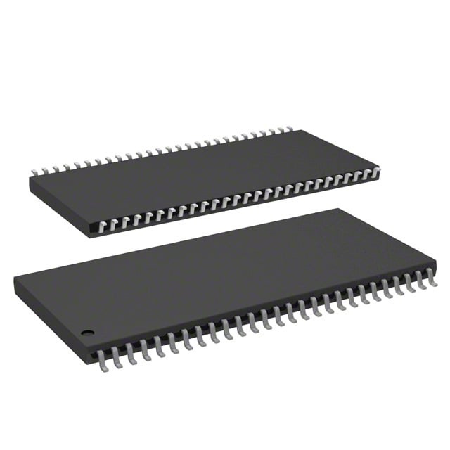
IC DRAM 512MBIT PAR 54TSOP II |
|---|---|
| Quantity | 1,006 Available (as of June 15, 2026) |

| Product Category | Memory |
|---|---|
| Manufacturer | Integrated Silicon Solution Inc |
| Manufacturing Status | Obsolete |
| Manufacturer Standard Lead Time | Contact Us |
| Datasheet |
Specifications & Environmental
| Device Package | 54-TSOP II | Memory Format | DRAM | Technology | SDRAM | ||
|---|---|---|---|---|---|---|---|
| Memory Size | 512 Mbit | Access Time | 5.4 ns | Grade | Industrial | ||
| Clock Frequency | 143 MHz | Voltage | 3V ~ 3.6V | Memory Type | Volatile | ||
| Operating Temperature | -40°C ~ 85°C (TA) | Write Cycle Time Word Page | N/A | Packaging | 54-TSOP (0.400", 10.16mm Width) | ||
| Mounting Method | Volatile | Memory Interface | Parallel | Memory Organization | 64M x 8 | ||
| Moisture Sensitivity Level | 3 (168 Hours) | RoHS Compliance | ROHS3 Compliant | REACH Compliance | REACH Unaffected | ||
| Qualification | N/A | ECCN | EAR99 | HTS Code | 8542.32.0028 |
Overview of IS42S86400D-7TLI-TR – IC DRAM 512MBIT PAR 54TSOP II
The IS42S86400D-7TLI-TR is a 512 Mbit synchronous DRAM organized as 64M × 8 that implements a pipeline architecture for high-speed data transfer. It is a fully synchronous, parallel-interface DRAM optimized for designs requiring predictable, clock-referenced memory access.
Designed for 3.0–3.6 V systems and rated for operation from −40°C to +85°C, this 54‑pin TSOP‑II packaged device provides configurable burst operation, internal banking for hidden row access/precharge, and standard SDRAM control primitives for refresh and latency management.
Key Features
- Core / Architecture Fully synchronous SDRAM with pipeline architecture; all inputs and outputs referenced to the rising edge of the clock and internal banks for hiding row access/precharge.
- Memory Density & Organization 512 Mbit capacity organized as 64M × 8 (16M × 8 × 4 banks), providing dense parallel memory in a compact footprint.
- Clock & Timing -7 speed grade supports a clock frequency of 143 MHz with CAS latency options of 2 or 3 clocks; typical access time from clock is 5.4 ns (CAS latency = 3).
- Burst & Transfer Control Programmable burst length (1, 2, 4, 8, full page) and selectable burst sequence (sequential or interleave) with burst termination via burst stop or precharge commands.
- Refresh & Self‑Management Supports Auto Refresh (CBR) and Self Refresh modes with 8K refresh cycles every 64 ms as specified.
- Interface & Signaling LVTTL-compatible interface and parallel memory interface for synchronous system integration.
- Power Voltage supply range specified at 3.0 V to 3.6 V.
- Package & Temperature 54‑pin TSOP‑II package (0.400", 10.16 mm width) with an operating ambient temperature range of −40°C to +85°C.
Typical Applications
- High‑speed memory buffering Used where clock‑referenced, pipelined data transfer and burst modes are required for temporary data storage and buffering.
- Synchronous system memory for embedded designs Provides parallel SDRAM capacity and predictable timing for embedded platforms that use synchronous DRAM interfaces.
- Pipeline data storage Suited for designs that leverage internal banking and hidden row access/precharge to maintain throughput in pipelined memory architectures.
Unique Advantages
- Synchronous pipeline architecture: Enables clock‑referenced data transfers and predictable timing behavior for systems that rely on deterministic memory access.
- Flexible burst control: Programmable burst lengths and selectable burst sequences let designers match transfer patterns to system throughput requirements.
- Internal banking for throughput: Multiple internal banks hide row access and precharge cycles to sustain higher effective data rates.
- Industrial temperature range: Rated for −40°C to +85°C, supporting deployment in temperature‑variable environments.
- Compact TSOP‑II packaging: 54‑pin TSOP‑II (10.16 mm width) delivers 512 Mbit density in a board‑area efficient form factor.
- Standard LVTTL interface: Simplifies integration with logic families that use LVTTL signaling for control and data lines.
Why Choose IS42S86400D-7TLI-TR?
The IS42S86400D-7TLI-TR combines a 512 Mbit SDRAM density with a fully synchronous, pipelined architecture and internal banking to provide predictable, high‑speed parallel memory for clocked digital systems. Its 143 MHz (-7) speed grade, programmable burst options, and LVTTL interface make it well suited to applications that require controlled timing, burst transfers, and efficient board footprint.
This device is appropriate for designers needing scalable SDRAM capacity with refresh management and self‑refresh support, delivered in a compact 54‑pin TSOP‑II package and qualified for operation across a −40°C to +85°C ambient range.
If you require pricing, lead time, or a formal quote for IS42S86400D-7TLI-TR, request a quote or submit an inquiry to obtain current availability and ordering information.