IS43DR16160A-5BBLI-TR
| Part Description |
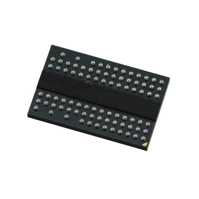
IC DRAM 256MBIT PAR 84TWBGA |
|---|---|
| Quantity | 1,571 Available (as of June 15, 2026) |

| Product Category | Memory |
|---|---|
| Manufacturer | Integrated Silicon Solution Inc |
| Manufacturing Status | Obsolete |
| Manufacturer Standard Lead Time | Contact Us |
| Datasheet |
Specifications & Environmental
| Device Package | 84-TWBGA (8x12.5) | Memory Format | DRAM | Technology | SDRAM - DDR2 | ||
|---|---|---|---|---|---|---|---|
| Memory Size | 256 Mbit | Access Time | 600 ps | Grade | Industrial | ||
| Clock Frequency | 200 MHz | Voltage | 1.7V ~ 1.9V | Memory Type | Volatile | ||
| Operating Temperature | -40°C ~ 85°C (TA) | Write Cycle Time Word Page | 15 ns | Packaging | 84-TFBGA | ||
| Mounting Method | Volatile | Memory Interface | Parallel | Memory Organization | 16M x 16 | ||
| Moisture Sensitivity Level | 3 (168 Hours) | RoHS Compliance | ROHS3 Compliant | REACH Compliance | REACH Unaffected | ||
| Qualification | N/A | ECCN | EAR99 | HTS Code | 8542.32.0024 |
Overview of IS43DR16160A-5BBLI-TR – 256Mbit DDR2 SDRAM, 16M × 16, 84-TWBGA
The IS43DR16160A-5BBLI-TR is a 256Mbit DDR2 SDRAM organized as 16M × 16 in an 84-ball thin wafer BGA (8 mm × 12.5 mm) package. It implements a double-data-rate architecture with on-chip DLL and a 4-bit prefetch to support high-rate data transfers on a parallel DDR2 interface.
Designed for board-level memory expansion where a compact, 1.8V-class parallel DRAM is required, this device provides programmable timing options and on-die features to address signal-integrity and performance tuning needs.
Key Features
- Core / Architecture Double-data-rate (DDR2) operation with 4-bit prefetch and an on-chip DLL to align DQ and DQS transitions with CK.
- Memory Organization 256 Mbit density organized as 16M × 16 with four internal banks for concurrent operation.
- Timing & Performance Programmable CAS latency (CL = 3, 4, 5, 6) and programmable additive latency (AL = 0–5). Supported burst lengths: 4 or 8. Listed timing parameters include tCK variants and typical tRCD/tRP values shown in the device timing table.
- Interface JEDEC-standard 1.8V I/O (SSTL_18-compatible) double-data-rate parallel interface with differential data strobe (DQS/ DQS̄).
- Signal Integrity On-die termination (ODT) and adjustable data-output drive strength to help optimize board-level signal quality.
- Power Nominal VDD/VDDQ = 1.8 V (specified 1.7 V to 1.9 V supply range).
- Performance Numbers Specified clock frequency 200 MHz with an access time of 600 ps and a typical write-cycle time (word page) of 15 ns.
- Package & Temperature 84-TWBGA (8 mm × 12.5 mm) package; ambient operating temperature range −40 °C to 85 °C.
Typical Applications
- Board-level memory expansion Provides a 256 Mbit parallel DDR2 SDRAM option where compact, 1.8V-class memory density is required on system boards.
- High-speed data buffering Suitable for designs that need DDR2 performance with programmable latencies and burst control for data buffering tasks.
- Compact, high-density modules The 84-ball WBGA package enables placement in space-constrained designs that require a 16M × 16 memory organization.
Unique Advantages
- Flexible timing configuration: Programmable CAS and additive latencies plus selectable burst lengths allow designers to tune performance to system timing requirements.
- Signal-integrity features: Differential DQS, on-chip DLL, on-die termination, and adjustable drive strength help optimize data capture and board-level signal quality.
- 1.8V SSTL-compatible I/O: Operates within a 1.7–1.9 V supply window, matching JEDEC 1.8 V I/O signaling expectations for DDR2 systems.
- Compact WBGA footprint: 84-TWBGA (8 mm × 12.5 mm) package provides a small, solderable package for high-density board integration.
- Wide operating range: Specified ambient operation from −40 °C to 85 °C supports deployment in varied temperature environments.
Why Choose IC DRAM 256MBIT PAR 84TWBGA?
The IS43DR16160A-5BBLI-TR delivers a straightforward, board-level DDR2 memory option with 256 Mbit density, programmable timing, and on-die features that support reliable high-speed operation. Its combination of differential DQS, DLL alignment, ODT and drive-strength options makes it suitable for designs that require tunable timing and improved signal integrity.
This device is appropriate for engineers specifying compact, parallel DDR2 memory in systems requiring a 16M × 16 organization and a small 84-ball WBGA footprint. The clear electrical and timing specifications enable predictable integration and tuning during memory subsystem design.
Request a quote or contact sales to discuss availability, lead times and pricing for the IS43DR16160A-5BBLI-TR.