IS43R16160D-5BL
| Part Description |
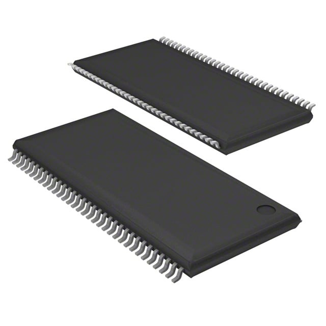
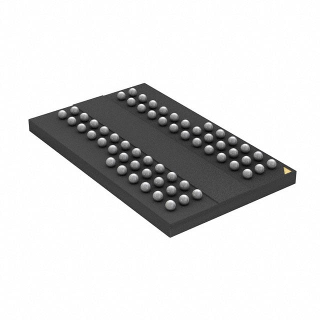
IC DRAM 256MBIT PAR 60TFBGA |
|---|---|
| Quantity | 109 Available (as of June 15, 2026) |
| Product Category | DRAM Memory |
|---|---|
| Manufacturer | Integrated Silicon Solution Inc |
| Manufacturing Status | Obsolete |
| Manufacturer Standard Lead Time | Contact Us |
| Datasheet |
Specifications & Environmental
| Device Package | 60-TFBGA (8x13) | Memory Format | DRAM | Technology | SDRAM - DDR | ||
|---|---|---|---|---|---|---|---|
| Memory Size | 256 Mbit | Access Time | 700 ps | Grade | Commercial | ||
| Clock Frequency | 200 MHz | Voltage | 2.3V ~ 2.7V | Memory Type | Volatile | ||
| Operating Temperature | 0°C ~ 70°C (TA) | Write Cycle Time Word Page | 15 ns | Packaging | 60-TFBGA | ||
| Mounting Method | Volatile | Memory Interface | Parallel | Memory Organization | 16M x 16 | ||
| Moisture Sensitivity Level | 3 (168 Hours) | RoHS Compliance | ROHS3 Compliant | REACH Compliance | REACH Unaffected | ||
| Qualification | N/A | ECCN | EAR99 | HTS Code | 8542.32.0024 |
Overview of IS43R16160D-5BL – IC DRAM 256Mbit PAR 60TFBGA
The IS43R16160D-5BL is a 256‑Mbit DDR SDRAM organized as 16M × 16 with a parallel memory interface in a 60‑TFBGA (8×13) package. It implements a double‑data‑rate architecture with on‑chip DLL and DQS support for high‑speed synchronous transfers.
Designed for systems requiring a 256‑Mbit parallel DDR memory device, the part supports up to 200 MHz clock operation (with programmable CAS latency), SSTL_2 compatible I/O and standard DDR features such as auto/self refresh and burst transfers.
Key Features
- Core / Memory 256‑Mbit DDR SDRAM organized as 16M × 16 with four internal banks for concurrent operation and pipelined Read/Write bursts.
- Double‑Data‑Rate Architecture Two data transfers per clock cycle with DQS transmitted/received alongside data; DQS is edge‑aligned for READs and center‑aligned for WRITEs.
- Clocking and Timing Differential clock inputs (CK / CK̅) and an on‑chip DLL to align DQ/DQS transitions with clock; typical maximum FCK up to 200 MHz (CL = 2.5 or 3).
- Interface and Protocol SSTL_2 compatible I/O, bidirectional data strobe (DQS), data mask (DM) that masks write data on both edges of DQS, and support for burst lengths 2, 4 and 8 with sequential and interleave modes.
- Power VDD and VDDQ nominal 2.5 V (2.3 V to 2.7 V supply range specified), matching SSTL_2 voltage requirements.
- Refresh and Power Management Auto Refresh and Self Refresh modes plus Auto Precharge support to maintain data integrity with low control overhead.
- Package & Thermal 60‑TFBGA (8×13) mounting package; commercial operating temperature range 0°C to +70°C.
- Performance Metrics Typical access characteristics include an access time on the order of 700 ps and a write cycle time/word page of 15 ns as specified.
Typical Applications
- Embedded memory subsystems Provides a 256‑Mbit parallel DDR SDRAM option (16M × 16) for designs requiring on‑board synchronous DRAM with SSTL_2 I/O.
- High‑speed buffering Double‑data‑rate transfers, DQS timing and on‑chip DLL enable burst read/write buffering at clock rates up to 200 MHz.
- Compact board designs 60‑TFBGA (8×13) package allows dense mounting where board space and signal integrity are considerations.
Unique Advantages
- DDR double‑data‑rate transfers: Two data transfers per clock cycle increase effective data throughput without increasing clock frequency.
- SSTL_2 compatible I/O: I/O voltage and signaling compatible with SSTL_2 standards (VDD/VDDQ 2.5 V nominal) for straightforward interface integration.
- Flexible timing options: Programmable CAS latency (2, 2.5, 3) and selectable burst lengths (2, 4, 8) allow tuning for system timing and throughput needs.
- Robust data capture: Bidirectional DQS with edge/center alignment and DLL support improves timing margin for both reads and writes.
- Power and refresh control: Auto Refresh and Self Refresh modes plus Auto Precharge reduce host CPU overhead for memory maintenance.
- Small BGA footprint: 60‑TFBGA (8×13) package supports compact board layouts while maintaining required pinout for parallel DDR operation.
Why Choose IS43R16160D-5BL?
The IS43R16160D-5BL combines standard DDR SDRAM features—double‑data‑rate transfers, DQS‑based data capture, on‑chip DLL and SSTL_2 I/O—with a 16M × 16 organization in a compact 60‑TFBGA package. Its 2.3 V–2.7 V supply range, programmable latencies and support for burst modes make it suitable for designs that need predictable DDR performance up to 200 MHz clock operation within a commercial temperature range (0°C to +70°C).
Manufactured by Integrated Silicon Solution Inc., this device is positioned for engineers specifying a 256‑Mbit parallel DDR memory component where board density, timing flexibility and standard DDR signaling are primary design considerations.
Request a quote or submit your RFQ to obtain pricing, availability and lead‑time information for the IS43R16160D-5BL.