IS43R16160D-5BLI
| Part Description |
IC DRAM 256MBIT PAR 60TFBGA |
|---|---|
| Quantity | 199 Available (as of June 9, 2026) |

| Product Category | Memory |
|---|---|
| Manufacturer | Integrated Silicon Solution Inc |
| Manufacturing Status | Obsolete |
| Manufacturer Standard Lead Time | Contact Us |
| Datasheet |
Specifications & Environmental
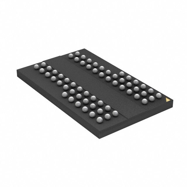
| Device Package | 60-TFBGA (8x13) | Memory Format | DRAM | Technology | SDRAM - DDR | ||
|---|---|---|---|---|---|---|---|
| Memory Size | 256 Mbit | Access Time | 700 ps | Grade | Industrial | ||
| Clock Frequency | 200 MHz | Voltage | 2.3V ~ 2.7V | Memory Type | Volatile | ||
| Operating Temperature | -40°C ~ 85°C (TA) | Write Cycle Time Word Page | 15 ns | Packaging | 60-TFBGA | ||
| Mounting Method | Volatile | Memory Interface | Parallel | Memory Organization | 16M x 16 | ||
| Moisture Sensitivity Level | 3 (168 Hours) | RoHS Compliance | ROHS Compliant | REACH Compliance | REACH Unaffected | ||
| Qualification | N/A | ECCN | EAR99 | HTS Code | 8542.32.0024 |
Overview of IS43R16160D-5BLI – IC DRAM 256MBIT PAR 60TFBGA
The IS43R16160D-5BLI is a 256 Mbit DDR SDRAM device organized as 16M × 16 with a parallel memory interface, supplied in a 60‑TFBGA (8×13) package. It uses a double-data-rate architecture with SSTL_2 compatible I/O and is designed for systems requiring high-throughput burst transfers and flexible timing options.
Typical use cases include embedded and system-level memory expansion where a 256 Mbit DDR SDRAM with programmable CAS latency, burst control and standard DDR features (DQS, DLL, differential clock inputs) is required. The device delivers timing and interface features that support sustained read/write bursts and common DDR memory operations.
Key Features
- Memory Core & Capacity 256 Mbit DDR SDRAM organized as 16M × 16 with four internal banks to enable concurrent operations across the device.
- DDR Architecture Double-data-rate operation supporting two data transfers per clock cycle; DQS is transmitted/received with data and is edge-aligned for READs and centre-aligned for WRITEs.
- I/O and Clock SSTL_2 compatible I/O with differential clock inputs (CK and /CK) and a DLL to align DQ/DQS transitions with clock edges; commands are registered on the positive CLK edge.
- Programmable Burst and Latency Burst Length options of 2, 4 and 8 with Sequential and Interleave modes; programmable CAS latencies of 2, 2.5 and 3 provide timing flexibility.
- Refresh and Power Modes Supports Auto Refresh and Self Refresh modes plus Auto Precharge to manage refresh and retention behavior.
- Timing and Performance Maximum clock frequency up to 200 MHz (speed grade -5); access time specified as 700 ps and write cycle time (word page) of 15 ns.
- Supply and Signaling VDD and VDDQ operate around 2.5 V (specified supply range 2.3 V to 2.7 V); Data Mask (DM) masks write data on both edges of the data strobe.
- Package and Temperature 60‑TFBGA (8×13) package option; industrial temperature range specified from -40 °C to +85 °C. Lead‑free package available per device options in the datasheet.
Typical Applications
- System Memory Expansion Use as a 256 Mbit parallel DDR SDRAM for embedded systems and modules requiring moderate-density DDR memory.
- High‑throughput Buffering Suitable for buffering and burst-oriented data paths that leverage DDR burst lengths and DQS-based data capture.
- Industrial Electronics Applicable in industrial equipment operating within -40 °C to +85 °C that require standard DDR timing and refresh management.
Unique Advantages
- DDR Double‑Data‑Rate Throughput Two data transfers per clock cycle increase effective bandwidth for burst read/write operations.
- SSTL_2 Compatible I/O Industry-standard signaling compatibility simplifies interfacing with SSTL_2 systems and controllers.
- Flexible Timing Configuration Programmable CAS latencies (2, 2.5, 3) and selectable burst lengths (2, 4, 8) allow designers to tune performance to system requirements.
- Robust Clock and Data Alignment DLL plus differential clock inputs and DQS alignment behavior support reliable data capture at both read and write operations.
- Industrial Temperature Range Specified operation from -40 °C to +85 °C supports deployment in a wide range of temperature environments.
- Compact BGA Package 60‑TFBGA (8×13) footprint provides a space-efficient mounting option for board-level designs.
Why Choose IC DRAM 256MBIT PAR 60TFBGA?
The IS43R16160D-5BLI provides a compact, 256 Mbit DDR SDRAM solution with standard DDR features—DQS, DLL, differential clocking and programmable latency—suitable for designs that require controlled timing, burst-oriented transfers and SSTL_2 signaling. Its 16M × 16 organization and four internal banks enable concurrent memory operations while the 60‑TFBGA package supports space-constrained board layouts.
This device is appropriate for engineers and integrators seeking a predictable DDR memory building block with defined timing options, industrial temperature capability and standard supply requirements (2.3 V–2.7 V). It offers long-term design utility where established DDR features and package density are required.
Request a quote or submit an inquiry for pricing and availability of the IS43R16160D-5BLI to evaluate it for your design and procurement needs.