IS43R16160D-6BL
| Part Description |
IC DRAM 256MBIT PAR 60TFBGA |
|---|---|
| Quantity | 761 Available (as of June 14, 2026) |

| Product Category | Memory |
|---|---|
| Manufacturer | Integrated Silicon Solution Inc |
| Manufacturing Status | Obsolete |
| Manufacturer Standard Lead Time | Contact Us |
| Datasheet |
Specifications & Environmental
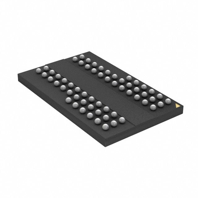
| Device Package | 60-TFBGA (8x13) | Memory Format | DRAM | Technology | SDRAM - DDR | ||
|---|---|---|---|---|---|---|---|
| Memory Size | 256 Mbit | Access Time | 700 ps | Grade | Commercial | ||
| Clock Frequency | 166 MHz | Voltage | 2.3V ~ 2.7V | Memory Type | Volatile | ||
| Operating Temperature | 0°C ~ 70°C (TA) | Write Cycle Time Word Page | 15 ns | Packaging | 60-TFBGA | ||
| Mounting Method | Volatile | Memory Interface | Parallel | Memory Organization | 16M x 16 | ||
| Moisture Sensitivity Level | 3 (168 Hours) | RoHS Compliance | ROHS Compliant | REACH Compliance | REACH Unaffected | ||
| Qualification | N/A | ECCN | EAR99 | HTS Code | 8542.32.0024 |
Overview of IS43R16160D-6BL – IC DRAM 256MBIT PAR 60TFBGA
The IS43R16160D-6BL is a 256 Mbit DDR SDRAM organized as 16M × 16, implemented in a parallel DRAM architecture with double-data-rate operation. The device uses a pipeline architecture with four internal banks and supports SSTL_2 compatible I/O, differential clock inputs, and a data strobe (DQS) for registered data capture.
Designed for systems that require high-speed, parallel DDR memory, the device delivers dual transfers per clock cycle and programmable timing options to match system timing requirements. Key attributes include a 60‑TFBGA (8×13) package, 2.3 V–2.7 V supply range, and an operating temperature range of 0°C to 70°C.
Key Features
- Core & Architecture Double-data-rate architecture with pipeline access and four internal banks for concurrent operation, enabling continuous read/write burst accesses.
- Memory Organization 256 Mbit capacity organized as 16M × 16, providing a parallel 16-bit data interface.
- Performance Supports up to 166 MHz clock frequency (device speed grade -6 listed at 167 MHz in timing table); programmable CAS latencies of 2, 2.5 and 3 and burst lengths of 2, 4 and 8.
- Data Timing & Capture Bidirectional data strobe (DQS) transmitted/received with data; DQS edge-aligned for READ and centre-aligned for WRITE operations. DLL aligns DQ/DQS with CK transitions.
- Interface & Commands Differential clock inputs (CK/CK̄) with commands registered on positive CK edges; data and data mask referenced to both edges of DQS.
- Refresh & Power Modes Auto Refresh and Self Refresh modes supported; Auto Precharge and TRAS lockout supported to manage row timing.
- Timing & Latency Access time listed as 700 ps and write cycle time (word/page) of 15 ns, enabling tight timing control for burst operations.
- Power VDD and VDDQ operation at 2.5 V ±0.2 V (specified supply range 2.3 V–2.7 V); SSTL_2 compatible I/O signaling.
- Package & Temperature Available in a 60‑TFBGA (8×13) package; commercial operating temperature range of 0°C to 70°C.
Typical Applications
- High‑speed memory subsystems Use where a 256 Mbit DDR SDRAM with burst capability and programmable CAS latency is required for throughput and buffering.
- Board‑level parallel DDR memory Suitable for PCB designs that require SSTL_2 compatible I/O and a compact 60‑TFBGA (8×13) package footprint.
- Systems requiring low-voltage DDR I/O Ideal for designs constrained to the 2.3 V–2.7 V supply range and commercial temperature operation.
Unique Advantages
- Double-data-rate transfers: Two data transfers per clock cycle increase data throughput without changing clock frequency.
- Flexible timing options: Programmable CAS latencies (2 / 2.5 / 3) and selectable burst lengths (2, 4, 8) allow tuning for a variety of system timing requirements.
- Robust data capture: Bidirectional DQS with DLL alignment and differential clocking improves timing margin for both reads and writes.
- Concurrent bank operation: Four internal banks support overlapping commands and burst accesses to improve effective memory efficiency.
- Compact package: 60‑TFBGA (8×13) package provides a small footprint for board-level integration.
- Standard supply and signaling: 2.5 V ±0.2 V VDD/VDDQ and SSTL_2 I/O compatibility simplify integration with SSTL_2 signaling systems.
Why Choose IC DRAM 256MBIT PAR 60TFBGA?
The IS43R16160D-6BL positions itself as a focused, standards-based DDR SDRAM device for designs that require a 256 Mbit parallel DDR memory with programmable latency, burst control, and SSTL_2 I/O. Its DLL-aligned DQ/DQS, differential clock inputs, and four-bank architecture support predictable burst behavior and concurrent operations.
This device is well suited to engineers specifying board-level DDR memory where a 16‑bit data interface, compact 60‑TFBGA package, and commercial temperature range (0°C to 70°C) meet system requirements. The combination of programmable timing, refresh modes, and supported supply range offers design flexibility for a variety of parallel DDR memory implementations.
Request a quote or contact sales to discuss availability, pricing, and lead times for the IS43R16160D-6BL.