IS43R16160D-6TL
| Part Description |
IC DRAM 256MBIT PAR 66TSOP II |
|---|---|
| Quantity | 826 Available (as of June 15, 2026) |

| Product Category | DRAM Memory |
|---|---|
| Manufacturer | Integrated Silicon Solution Inc |
| Manufacturing Status | Obsolete |
| Manufacturer Standard Lead Time | Contact Us |
| Datasheet |
Specifications & Environmental
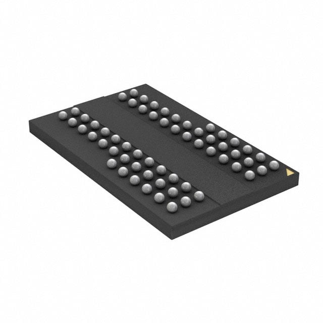
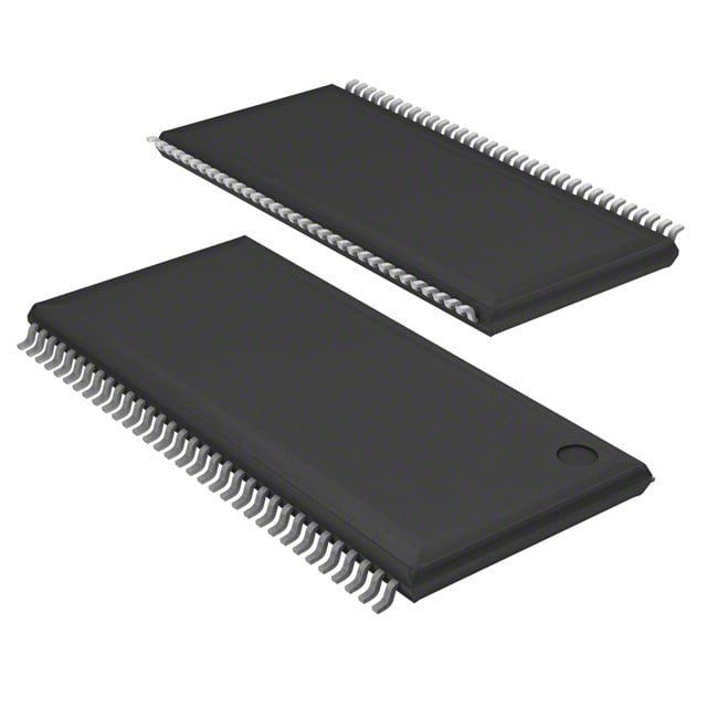
| Device Package | 66-TSOP II | Memory Format | DRAM | Technology | SDRAM - DDR | ||
|---|---|---|---|---|---|---|---|
| Memory Size | 256 Mbit | Access Time | 700 ps | Grade | Commercial | ||
| Clock Frequency | 166 MHz | Voltage | 2.3V ~ 2.7V | Memory Type | Volatile | ||
| Operating Temperature | 0°C ~ 70°C (TA) | Write Cycle Time Word Page | 15 ns | Packaging | 66-TSSOP (0.400", 10.16mm Width) | ||
| Mounting Method | Volatile | Memory Interface | Parallel | Memory Organization | 16M x 16 | ||
| Moisture Sensitivity Level | 3 (168 Hours) | RoHS Compliance | ROHS Compliant | REACH Compliance | REACH Unaffected | ||
| Qualification | N/A | ECCN | EAR99 | HTS Code | 8542.32.0024 |
Overview of IS43R16160D-6TL – IC DRAM 256MBIT PAR 66TSOP II
The IS43R16160D-6TL is a 256‑Mbit DDR SDRAM organized as 16M × 16 with a parallel memory interface. It implements a double‑data‑rate pipeline architecture with four internal banks to support high‑throughput burst read/write operations.
Designed for commercial temperature designs, the device targets systems that require externally accessible DDR memory with programmable latency, burst control and SSTL_2 compatible I/O signaling. Key value comes from its DDR throughput, flexible timing options and compact 66‑TSSOP (TSOP‑II) package.
Key Features
- Memory Architecture — 256 Mbit DRAM organized as 16M × 16 with four internal banks to enable concurrent operations and pipelined read/write bursts.
- Double‑Data‑Rate Operation — DDR architecture performs two data transfers per clock cycle, with data strobe (DQS) used for capture and differential clock inputs (CK/CK̄).
- Programmable Burst and Latency — Burst length options of 2, 4 and 8 and programmable CAS latency of 2, 2.5 and 3 support flexible performance/latency tradeoffs.
- Data Timing and Integrity — DLL aligns DQ/DQS with clock edges; DQS is edge‑aligned for reads and center‑aligned for writes; Data Mask (DM) masks write data on both edges of DQS.
- Signal Compatibility — SSTL_2 compatible I/O for standard DDR signaling requirements.
- Performance Parameters — Rated clock frequency up to 166 MHz (speed grade -6), typical access time 700 ps and write cycle time (word/page) of 15 ns.
- Power — VDD and VDDQ operating range from 2.3 V to 2.7 V (datasheet nominal 2.5 V ±0.2 V).
- Package and Temperature — Available in 66‑pin TSOP‑II / 66‑TSSOP package (0.400", 10.16 mm width); commercial operating temperature 0°C to +70°C.
- Refresh and Power Modes — Supports Auto Refresh and Self Refresh modes as well as Auto Precharge for standard DRAM refresh management.
Typical Applications
- Embedded memory subsystems — External DDR memory for embedded controllers and peripherals that require parallel DDR SDRAM capacity and burst access control.
- Consumer and commercial electronics — Buffering and high‑speed temporary storage in commercial temperature‑range designs where 256‑Mbit DDR is appropriate.
- Memory expansion modules — Integration into memory expansion boards or modules that require a compact 66‑TSSOP footprint and SSTL_2 compatible signaling.
Unique Advantages
- Higher throughput via DDR transfers: Two data transfers per clock cycle increase effective data rate compared with single‑edge SDR devices.
- Flexible timing control: Programmable CAS latency (2 / 2.5 / 3) and selectable burst lengths (2, 4, 8) let designers tune performance and latency.
- SSTL_2 compatible I/O: Enables straightforward interfacing with standard DDR signaling domains.
- Concurrent bank operation: Four internal banks and pipelined architecture support overlapping commands and near‑continuous burst accesses.
- Compact package: 66‑TSSOP (TSOP‑II) package provides a small PCB footprint (0.400", 10.16 mm width) for space‑constrained designs.
- Low voltage operation: 2.3 V to 2.7 V supply range (nominal 2.5 V) reduces supply requirements compared to older higher‑voltage memories.
Why Choose IS43R16160D-6TL?
The IS43R16160D-6TL positions itself as a versatile 256‑Mbit DDR SDRAM solution for designs that require parallel DDR memory with programmable latency, burst control and SSTL_2 signaling. Its pipelined DDR architecture and four‑bank organization enable sustained burst throughput while the compact 66‑TSSOP package supports dense PCB implementations.
This device is suited for engineers and procurement teams specifying commercial temperature‑range external memory where predictable timing (access time, write cycle) and flexible burst/latency settings are important. The combination of DDR transfer rates, low‑voltage operation and package density provides a balance of performance and board‑level integration for a range of commercial applications.
If you would like pricing, availability or a formal quote for IS43R16160D-6TL, submit a request for a quote or contact sales for ordering and lead‑time details.