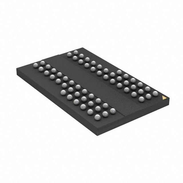
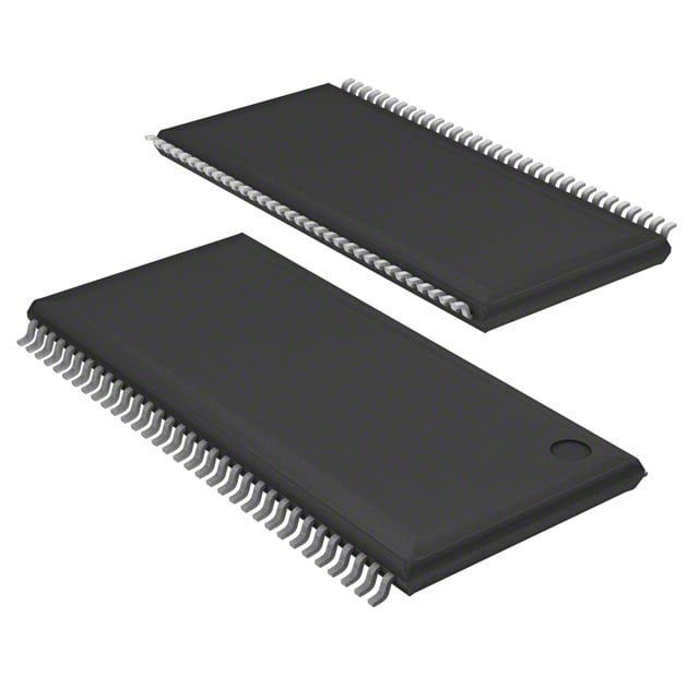
IS43R16160D-6TLI-TR
| Part Description |
IC DRAM 256MBIT PAR 66TSOP II |
|---|---|
| Quantity | 541 Available (as of June 15, 2026) |

| Product Category | Memory |
|---|---|
| Manufacturer | Integrated Silicon Solution Inc |
| Manufacturing Status | Obsolete |
| Manufacturer Standard Lead Time | Contact Us |
| Datasheet |
Specifications & Environmental
| Device Package | 66-TSOP II | Memory Format | DRAM | Technology | SDRAM - DDR | ||
|---|---|---|---|---|---|---|---|
| Memory Size | 256 Mbit | Access Time | 700 ps | Grade | Industrial | ||
| Clock Frequency | 166 MHz | Voltage | 2.3V ~ 2.7V | Memory Type | Volatile | ||
| Operating Temperature | -40°C ~ 85°C (TA) | Write Cycle Time Word Page | 15 ns | Packaging | 66-TSSOP (0.400", 10.16mm Width) | ||
| Mounting Method | Volatile | Memory Interface | Parallel | Memory Organization | 16M x 16 | ||
| Moisture Sensitivity Level | 3 (168 Hours) | RoHS Compliance | ROHS Compliant | REACH Compliance | REACH Unaffected | ||
| Qualification | N/A | ECCN | EAR99 | HTS Code | 8542.32.0024 |
Overview of IS43R16160D-6TLI-TR – 256Mbit DDR SDRAM, 66‑TSOP II
The IS43R16160D-6TLI-TR is a 256‑Mbit DDR SDRAM organized as 16M × 16, implemented in a 66‑pin TSOP‑II package. It uses a double‑data‑rate architecture with a pipeline design and four internal banks to support high‑speed burst read/write operations.
Designed for applications that require high data throughput and predictable timing, this device provides SSTL_2 compatible I/O, differential clock inputs, and programmable burst and CAS timing options. The device is specified for VDD/VDDQ at 2.5 V ±0.2 V (2.3 V–2.7 V) and an operating temperature range of −40°C to +85°C.
Key Features
- Core Architecture Double‑data‑rate SDRAM with pipeline architecture enabling two data transfers per clock cycle and four internal banks for concurrent operation.
- Memory Organization 256 Mbit capacity arranged as 16M × 16 bits, suitable for 16‑bit parallel interfaces.
- High‑speed Timing Clock frequency up to 166 MHz (speed grade -6), programmable CAS latencies 2, 2.5 and 3, and access time of 700 ps; write cycle time (word/page) specified at 15 ns.
- Data Path and Clocking SSTL_2 compatible I/O, bidirectional data strobe (DQS) for capture alignment, DQS edge‑aligned for reads and centre‑aligned for writes, and differential clock inputs (CK/CK̄).
- Signal Integrity and Timing Control On‑die DLL aligns DQ/DQS with CK; commands are registered on positive CLK edges and data is referenced to both edges of DQS.
- Burst and Masking Burst lengths of 2, 4 and 8 with sequential and interleave modes; data mask (DM) supports masking at both rising and falling edges of DQS.
- Power and Voltage VDD and VDDQ specified at 2.5 V ±0.2 V (2.3 V–2.7 V).
- Package and Temperature 66‑TSSOP (0.400", 10.16 mm width) TSOP‑II package; operating temperature range −40°C to +85°C.
- Refresh and Power Modes Auto Refresh and Self Refresh supported, plus Auto Precharge and TRAS lockout (tRAP = tRCD).
Typical Applications
- High‑speed memory subsystems For designs that require double‑data‑rate transfers and burst access to sustain high throughput.
- Concurrent bank operation designs Systems needing multiple bank interleaving to improve sustained access efficiency.
- Systems requiring SSTL_2 I/O Applications that depend on SSTL_2 compatible signaling and differential clock inputs for timing integrity.
- Temperature‑sensitive embedded designs Equipment operating across −40°C to +85°C that requires a compact 66‑TSOP II memory package.
Unique Advantages
- Double‑data‑rate throughput: Two data transfers per clock cycle increase effective bandwidth without raising clock frequency.
- Flexible burst control: Selectable burst lengths (2/4/8) and burst types (sequential/interleave) allow tuning for access patterns and system latency.
- SSTL_2 and DQS support: SSTL_2 compatible I/O with bidirectional DQS and DLL alignment improves capture reliability at high data rates.
- Programmable timing: CAS latency options (2, 2.5, 3) provide tradeoffs between latency and maximum clock rate for system optimization.
- Compact package with industrial temp range: 66‑TSSOP (TSOP‑II) package delivers a space‑efficient footprint while supporting −40°C to +85°C operation.
Why Choose IC DRAM 256MBIT PAR 66TSOP II?
The IS43R16160D-6TLI-TR combines DDR SDRAM performance features—double‑data‑rate transfers, DQS timing, DLL alignment and programmable latency—with a compact 66‑TSSOP package and industrial temperature rating. Its 16M × 16 organization and SSTL_2 I/O make it suitable for designs that require parallel 16‑bit data paths and reliable timing at up to the specified clock frequency.
This device is appropriate for engineers and system designers who need predictable burst performance, flexible timing configuration, and a documented voltage and thermal envelope. Backed by detailed device specification, it supports integration into systems where controlled DDR timing and compact packaging are priorities.
Request a quote or submit a request for pricing and availability to receive technical and purchasing information for the IS43R16160D-6TLI-TR.