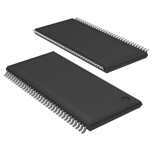
IS43R16160D-6TL-TR
| Part Description |
IC DRAM 256MBIT PAR 66TSOP II |
|---|---|
| Quantity | 1,207 Available (as of June 15, 2026) |
| Product Category | Memory |
|---|---|
| Manufacturer | Integrated Silicon Solution Inc |
| Manufacturing Status | Obsolete |
| Manufacturer Standard Lead Time | Contact Us |
| Datasheet |
Specifications & Environmental
| Device Package | 66-TSOP II | Memory Format | DRAM | Technology | SDRAM - DDR | ||
|---|---|---|---|---|---|---|---|
| Memory Size | 256 Mbit | Access Time | 700 ps | Grade | Commercial | ||
| Clock Frequency | 166 MHz | Voltage | 2.3V ~ 2.7V | Memory Type | Volatile | ||
| Operating Temperature | 0°C ~ 70°C (TA) | Write Cycle Time Word Page | 15 ns | Packaging | 66-TSSOP (0.400", 10.16mm Width) | ||
| Mounting Method | Volatile | Memory Interface | Parallel | Memory Organization | 16M x 16 | ||
| Moisture Sensitivity Level | 3 (168 Hours) | RoHS Compliance | ROHS3 Compliant | REACH Compliance | REACH Unaffected | ||
| Qualification | N/A | ECCN | EAR99 | HTS Code | 8542.32.0024 |
Overview of IS43R16160D-6TL-TR – IC DRAM 256MBIT PAR 66TSOP II
The IS43R16160D-6TL-TR is a 256 Mbit DDR SDRAM organized as 16M × 16 with a parallel memory interface in a 66‑pin TSOP‑II package. It uses a double‑data‑rate architecture with internal DLL and DQS signaling to support high‑speed bidirectional transfers for compact, board‑level memory subsystems.
Designed for commercial‑temperature applications, the device delivers programmable timing and burst options with low‑voltage operation (2.3 V–2.7 V), making it suitable for systems that require predictable DDR performance in a small footprint.
Key Features
- Core Architecture Double‑data‑rate (DDR) architecture enabling two data transfers per clock cycle; internal DLL aligns DQ/DQS with clock edges.
- Memory Organization 256 Mbit capacity arranged as 16M × 16 with four internal banks for concurrent operations and flexible addressing.
- Performance & Timing Rated for up to 166 MHz clock frequency (speed grade -6); programmable CAS latencies of 2, 2.5 and 3; burst lengths of 2, 4 and 8; write cycle time (word page) 15 ns; access time 700 ps.
- Interfaces & Signaling Parallel memory interface with SSTL_2 compatible I/O; bidirectional DQS transmitted/received with data, DQS edge‑aligned for READs and center‑aligned for WRITEs; differential clock inputs (CK/CK¯).
- Power Low‑voltage operation with VDD/VDDQ in the 2.3 V–2.7 V range (VDD and VDDQ: 2.5 V ±0.2 V).
- Refresh & Power Management Supports Auto Refresh and Self Refresh modes plus Auto Precharge for standard DRAM power management and data retention.
- Package & Temperature 66‑TSSOP (66‑TSOP II) package (0.400", 10.16 mm width); commercial operating temperature 0°C to +70°C.
- Data Integrity Controls Data Mask (DM) for write masking at both edges of the data strobe; TRAS lockout supported.
Typical Applications
- Embedded memory subsystems Parallel 16‑bit DDR memory for board‑level designs that require compact DRAM in a 66‑pin TSOP‑II package.
- High‑speed buffering and frame storage DDR architecture with burst lengths and DQS‑aligned transfers enables continuous read/write burst operation at system clock rates up to 166 MHz.
- Commercial electronic systems Commercial temperature range (0°C to +70°C) and low‑voltage operation make the device suitable for a range of commercial applications needing 256 Mbit of DDR SDRAM.
Unique Advantages
- Double‑data‑rate throughput: Two data transfers per clock cycle increase effective data bandwidth without increasing clock frequency.
- Flexible timing and burst control: Programmable CAS latencies (2 / 2.5 / 3) and selectable burst lengths (2 / 4 / 8) allow designers to tune performance to system requirements.
- Robust data capture: Bidirectional DQS with edge/center alignment plus DLL improves timing margin for both reads and writes.
- Low‑voltage operation: 2.3 V–2.7 V supply range (VDD/VDDQ: 2.5 V ±0.2 V) supports power‑sensitive designs.
- Compact package: 66‑TSSOP (TSOP‑II) provides a small PCB footprint for space‑constrained layouts.
- Concurrent bank operation: Four internal banks enable overlapped access sequences for improved throughput in burst workloads.
Why Choose IS43R16160D-6TL-TR?
The IS43R16160D-6TL-TR offers a balanced combination of DDR performance, low‑voltage operation, and a compact 66‑TSSOP package for designs that require 256 Mbit of parallel DDR SDRAM. Its programmable timing, DQS alignment, and internal bank architecture provide designers with the control needed to optimize throughput and latency for embedded and commercial applications.
Engineers specifying this device benefit from clearly defined electrical and timing characteristics—such as the 2.3 V–2.7 V supply range, up to 166 MHz clocking, and commercial temperature rating—making it a practical choice for board‑level memory subsystems where footprint and predictable DDR behavior are important.
If you need pricing, availability, or lead‑time information for IS43R16160D-6TL-TR, request a quote or submit an inquiry and our team will respond with the details you need.