IS43R16160D-5TLI
| Part Description |
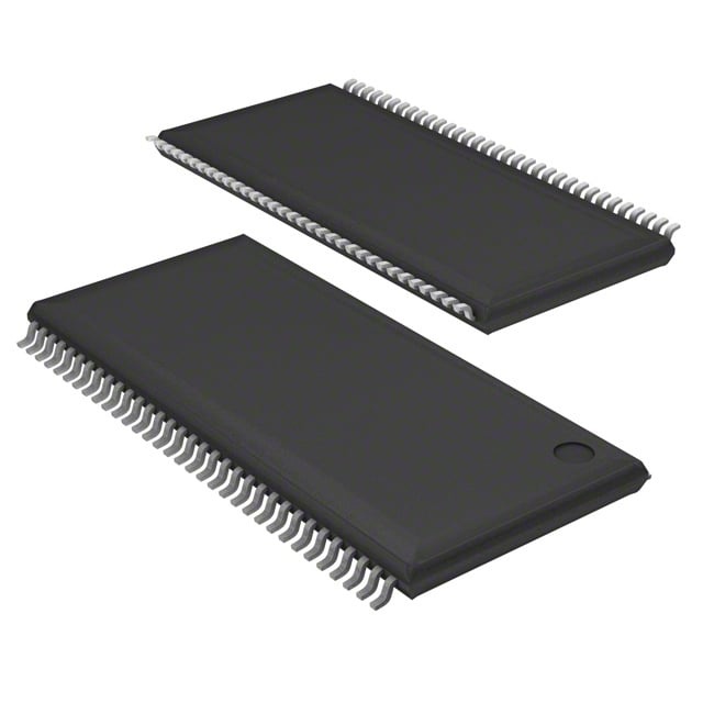
IC DRAM 256MBIT PAR 66TSOP II |
|---|---|
| Quantity | 1,216 Available (as of June 15, 2026) |

| Product Category | Memory |
|---|---|
| Manufacturer | Integrated Silicon Solution Inc |
| Manufacturing Status | Obsolete |
| Manufacturer Standard Lead Time | Contact Us |
| Datasheet |
Specifications & Environmental
| Device Package | 66-TSOP II | Memory Format | DRAM | Technology | SDRAM - DDR | ||
|---|---|---|---|---|---|---|---|
| Memory Size | 256 Mbit | Access Time | 700 ps | Grade | Industrial | ||
| Clock Frequency | 200 MHz | Voltage | 2.3V ~ 2.7V | Memory Type | Volatile | ||
| Operating Temperature | -40°C ~ 85°C (TA) | Write Cycle Time Word Page | 15 ns | Packaging | 66-TSSOP (0.400", 10.16mm Width) | ||
| Mounting Method | Volatile | Memory Interface | Parallel | Memory Organization | 16M x 16 | ||
| Moisture Sensitivity Level | 3 (168 Hours) | RoHS Compliance | ROHS3 Compliant | REACH Compliance | REACH Unaffected | ||
| Qualification | N/A | ECCN | EAR99 | HTS Code | 8542.32.0024 |
Overview of IS43R16160D-5TLI – IC DRAM 256MBIT PAR 66TSOP II
The IS43R16160D-5TLI is a 256 Mbit DDR SDRAM organized as 16M × 16 that implements a double-data-rate architecture for two data transfers per clock cycle. It provides a parallel memory interface with SSTL_2 compatible I/O, differential clock inputs and internal DLL support to align data and strobe signals for reliable high-speed operation.
Designed for systems that require low-latency burst access and industrial-temperature operation, this device delivers programmable latency and burst options, four internal banks for concurrent operations, and a compact 66‑TSOP II package for space-constrained board designs.
Key Features
- Core / Architecture Double-data-rate (DDR) SDRAM with pipeline architecture enabling two data transfers per clock cycle; internal DLL aligns DQ/DQS with CK.
- Memory Organization & Capacity 256 Mbit capacity organized as 16M × 16, implemented as four internal banks for concurrent operations.
- Interface & Data Strobe Parallel memory interface with SSTL_2 compatible I/O; bidirectional data strobe (DQS) is transmitted/received with data and used for capture at the receiver.
- Clock & Timing Differential clock inputs (CK and CK̄); maximum clock frequency up to 200 MHz (speed grade -5). Access time specified at 700 ps and programmable CAS latency options of 2, 2.5 and 3.
- Burst & Command Features Burst lengths of 2, 4 and 8 with sequential and interleave modes; commands registered on positive CK edge; Auto Refresh, Self Refresh and Auto Precharge supported.
- Write/Data Mask Data Mask (DM) supports masking of write data at both edges of the data strobe; write cycle time (word page) specified at 15 ns.
- Power Supply voltage range 2.3 V to 2.7 V (VDD/VDDQ nominal 2.5 V ±0.2 V as noted in device documentation).
- Package & Temperature Range Available in a 66‑pin TSOP‑II (66‑TSSOP, 0.400" / 10.16 mm width) package; operating temperature range −40°C to +85°C (TA).
Typical Applications
- High-speed buffering — For systems requiring low-latency burst transfers and continuous read/write burst accesses using DDR SDRAM architecture.
- 16-bit parallel memory systems — Direct replacement or integration where a 16M × 16, 256 Mbit DDR memory device is required.
- Industrial-temperature designs — Memory subsystems that must operate across −40°C to +85°C ambient conditions.
Unique Advantages
- Double-data-rate throughput: Delivers two data transfers per clock cycle for improved bandwidth compared with single-rate memories.
- Synchronized DQS and DLL support: Edge- and centre-aligned DQS with DLL alignment improve data capture reliability at high clock rates.
- Flexible timing and bursts: Programmable CAS latencies and selectable burst lengths (2/4/8) enable tuning for latency or throughput in target systems.
- Concurrent bank operation: Four internal banks allow overlapping commands and improve effective memory throughput for burst-oriented workloads.
- Compact package footprint: 66‑TSOP II package (10.16 mm width) helps reduce board area in constrained layouts.
- Industrial temperature support: Specified operation from −40°C to +85°C for deployment in temperature-challenging environments.
Why Choose IS43R16160D-5TLI?
The IS43R16160D-5TLI positions itself as a compact, parallel DDR SDRAM solution for designs that need 256 Mbit capacity, 16-bit data width, and configurable timing to balance latency and throughput. Its DDR architecture, DQS/DLL alignment and four-bank organization support continuous burst transfers and concurrent operations.
This device is suited to engineering teams and procurement looking for a robust memory component with industrial temperature capability, flexible burst and latency settings, and a small TSOP‑II footprint for space-constrained boards.
Request a quote or submit an inquiry to obtain pricing and lead-time information for the IS43R16160D-5TLI.