IS43R16320D-6TL
| Part Description |
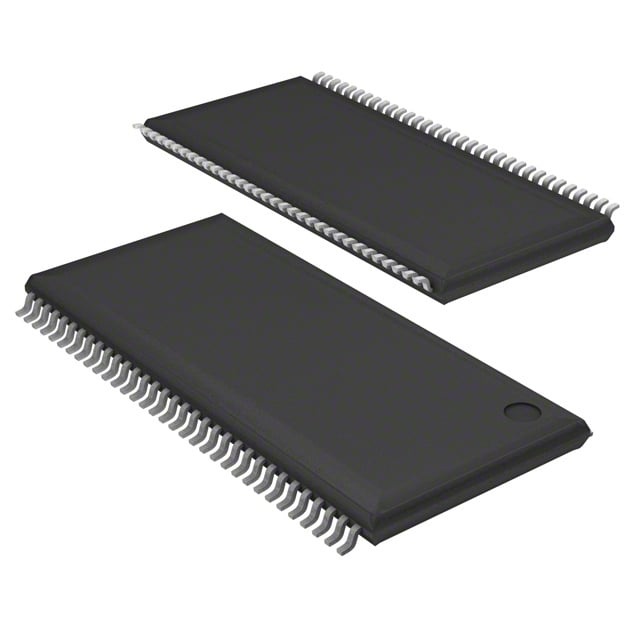
IC DRAM 512MBIT PAR 66TSOP II |
|---|---|
| Quantity | 1,977 Available (as of June 15, 2026) |

| Product Category | Memory |
|---|---|
| Manufacturer | Integrated Silicon Solution Inc |
| Manufacturing Status | Obsolete |
| Manufacturer Standard Lead Time | Contact Us |
| Datasheet |
Specifications & Environmental
| Device Package | 66-TSOP II | Memory Format | DRAM | Technology | SDRAM - DDR | ||
|---|---|---|---|---|---|---|---|
| Memory Size | 512 Mbit | Access Time | 700 ps | Grade | Commercial | ||
| Clock Frequency | 166 MHz | Voltage | 2.3V ~ 2.7V | Memory Type | Volatile | ||
| Operating Temperature | 0°C ~ 70°C (TA) | Write Cycle Time Word Page | 15 ns | Packaging | 66-TSSOP (0.400", 10.16mm Width) | ||
| Mounting Method | Volatile | Memory Interface | Parallel | Memory Organization | 32M x 16 | ||
| Moisture Sensitivity Level | 3 (168 Hours) | RoHS Compliance | ROHS3 Compliant | REACH Compliance | REACH Unaffected | ||
| Qualification | N/A | ECCN | EAR99 | HTS Code | 8542.32.0028 |
Overview of IS43R16320D-6TL – IC DRAM 512MBIT PAR 66TSOP II
The IS43R16320D-6TL is a 512‑Mbit DDR SDRAM device organized as 32M × 16 with a parallel memory interface. It implements a double‑data‑rate architecture with on‑chip DLL, differential clock inputs and DQS signaling to support high‑speed burst transfers and edge‑aligned data capture.
Designed for board‑level memory expansion, the device provides programmable burst lengths and CAS latencies, four internal banks for concurrent operations, and SSTL_2 compatible I/O in a compact 66‑TSOP II package.
Key Features
- Memory Core 512 Mbit DDR SDRAM organized as 32M × 16 with four internal banks to allow concurrent operations and continuous read/write burst access.
- DDR Architecture Double‑data‑rate design supporting two data transfers per clock cycle, differential clock inputs and an on‑chip DLL to align DQ/DQS with clock transitions.
- Data Strobe and Mask Bidirectional DQS transmitted/received with data (edge‑aligned for READs, centre‑aligned for WRITEs) and Data Mask (DM) that masks write data on both DQS edges.
- Programmable Burst and Latency Burst lengths of 2, 4 and 8 with sequential and interleave burst types; programmable CAS latency options of 2, 2.5 and 3.
- Performance / Timing Clock frequency up to approximately 166 MHz (-6 speed grade), access time of 700 ps and write cycle time (word page) of 15 ns.
- Voltage and I/O Standard VDD and VDDQ supported at 2.3 V to 2.7 V (VDD/VDDQ: 2.5 V ± 0.2 V for -6 grade); all I/Os are SSTL_2 compatible.
- Refresh and Power Modes Supports Auto Refresh and Self Refresh modes and Auto Precharge for memory management and power handling.
- Package and Temperature Available in a 66‑TSSOP (TSOP II) package (0.400", 10.16 mm width) with an operating temperature range of 0°C to 70°C (TA).
Typical Applications
- Board‑level memory expansion — Provides 512‑Mbit DDR storage for systems requiring a 16‑bit parallel DDR interface in a compact TSOP II footprint.
- Burst‑oriented buffering — Suited for designs that use contiguous read/write bursts and benefit from programmable burst lengths and CAS latency options.
- Performance‑sensitive embedded systems — Useful where DDR timing features (DLL, DQS, differential CLK) and SSTL_2 I/O are required to meet data capture timing.
Unique Advantages
- High‑throughput DDR operation: Two data transfers per clock cycle and differential CLK/DQS support increase effective data bandwidth for burst transfers.
- Flexible timing control: Programmable CAS latencies (2, 2.5, 3) and selectable burst lengths (2, 4, 8) let designers tune latency and throughput for system requirements.
- Concurrent bank operation: Four internal banks enable overlapped operations to improve effective access efficiency for interleaved memory access patterns.
- SSTL_2 compatible I/O and low‑voltage operation: VDD/VDDQ range of 2.3 V–2.7 V with SSTL_2 I/O compatibility supports standard DDR interface signaling and low‑voltage designs.
- Compact package: 66‑TSSOP (TSOP II) package provides a small footprint option for space‑constrained board designs.
Why Choose IS43R16320D-6TL?
The IS43R16320D-6TL delivers DDR SDRAM performance in a compact 66‑TSOP II package, combining double‑data‑rate transfers, DQS/DLL timing control and flexible burst/latency programming. Its 32M × 16 organization and four‑bank architecture make it suitable for systems that require efficient, burst‑oriented memory with SSTL_2 compatible I/O.
This device is appropriate for designers needing a 512‑Mbit parallel DDR memory building block with defined timing options, low‑voltage operation and standard commercial temperature range, offering a clear specification set for integration into board‑level memory subsystems.
Request a quote or contact sales to discuss availability, lead times and pricing for IS43R16320D-6TL.