IS43R32160D-5BLI
| Part Description |
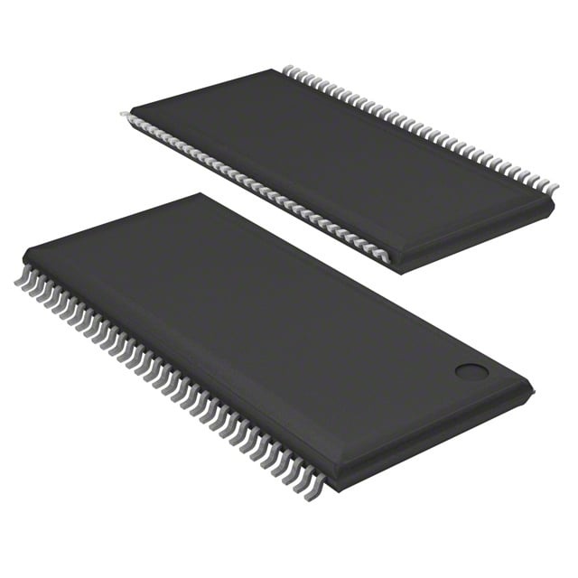
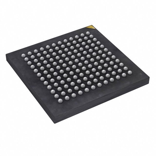
IC DRAM 512MBIT PAR 144LFBGA |
|---|---|
| Quantity | 905 Available (as of June 18, 2026) |

| Product Category | DRAM Memory |
|---|---|
| Manufacturer | Integrated Silicon Solution Inc |
| Manufacturing Status | Active |
| Manufacturer Standard Lead Time | 24 Weeks |
| Datasheet |
Specifications & Environmental
| Device Package | 144-LFBGA (12x12) | Memory Format | DRAM | Technology | SDRAM - DDR | ||
|---|---|---|---|---|---|---|---|
| Memory Size | 512 Mbit | Access Time | 700 ps | Grade | Industrial | ||
| Clock Frequency | 200 MHz | Voltage | 2.5V ~ 2.7V | Memory Type | Volatile | ||
| Operating Temperature | -40°C ~ 85°C (TA) | Write Cycle Time Word Page | 15 ns | Packaging | 144-LFBGA | ||
| Mounting Method | Volatile | Memory Interface | Parallel | Memory Organization | 16M x 32 | ||
| Moisture Sensitivity Level | 3 (168 Hours) | RoHS Compliance | ROHS3 Compliant | REACH Compliance | REACH Unaffected | ||
| Qualification | N/A | ECCN | EAR99 | HTS Code | 8542.32.0028 |
Overview of IS43R32160D-5BLI – IC DRAM 512MBIT PAR 144LFBGA
The IS43R32160D-5BLI is a 512‑Mbit DDR SDRAM device organized as 16M × 32 with a parallel memory interface in a 144‑LFBGA (12×12) package. It implements double‑data‑rate architecture with a DLL and differential clock inputs to support high‑speed, burst‑oriented memory transfers.
Designed for systems that require parallel DDR memory with programmable latency and burst options, the device delivers tiered timing and power options including a voltage supply range of 2.5 V to 2.7 V and an operating temperature of -40°C to +85°C (TA).
Key Features
- Memory Core and Organization 512 Mbit capacity organized as 16M × 32 with four internal banks for concurrent operations and a 536,870,912‑bit array.
- DDR Architecture Double‑data‑rate operation with two data transfers per clock cycle, bidirectional data strobe (DQS) and DLL alignment for reliable read/write timing.
- Clock and Timing Differential clock inputs (CK / CK̄), commands registered on the positive CK edge, programmable CAS latencies (2, 2.5, 3) and supported burst lengths of 2, 4 and 8. Speed grade -5 supports Fck up to 200 MHz at CL = 3.
- Interface and I/O SSTL_2 compatible I/O, DQS transmitted/received with data (edge‑aligned for reads, centre‑aligned for writes) and data mask (DM) that masks write data on both edges of DQS.
- Refresh and Power Modes Auto Refresh and Self Refresh modes plus Auto Precharge support to manage data integrity and power in idle conditions.
- Electrical and Timing Parameters Voltage supply range 2.5 V – 2.7 V (VDD/VDDQ specified for -5 grade at 2.6 V ± 0.1 V), typical access timing features include 700 ps access time and 15 ns write cycle time (word/page).
- Package and Temperature 144‑LFBGA (12×12) package; specified operating temperature range −40°C to +85°C (TA).
Typical Applications
- Embedded Memory Subsystems — Acts as on‑board parallel DDR storage for designs that require moderate density, burstable memory access.
- Communication and Networking Modules — Supports buffer and packet processing tasks that benefit from DDR burst transfers and low latency options.
- Consumer and Industrial Devices — Suitable for systems operating across −40°C to +85°C that need 512‑Mbit DDR memory in a compact LFBGA footprint.
Unique Advantages
- High‑throughput DDR transfers: Double‑data‑rate architecture with differential clock and DQS support provides two data transfers per clock cycle for increased bandwidth.
- Flexible timing control: Programmable CAS latencies and selectable burst lengths let designers balance latency and throughput per application needs.
- SSTL_2 compatible I/O: Industry standard signaling compatibility simplifies integration with SSTL_2 driven memory controllers.
- Robust operating range: Specified for −40°C to +85°C, enabling deployment across a wide range of environmental conditions.
- Compact LFBGA package: 144‑ball 12×12 LFBGA reduces board footprint while providing the required pinout for a 32‑bit parallel interface.
Why Choose IS43R32160D-5BLI?
The IS43R32160D-5BLI provides a balanced DDR SDRAM solution for designs that require 512‑Mbit density, parallel 32‑bit data paths and configurable timing behavior. Its DDR architecture, DQS/DLL timing support and SSTL_2 I/O compatibility make it suitable for systems that need predictable burst transfers and flexible latency settings.
With a defined supply range of 2.5 V–2.7 V, speed grade supporting up to 200 MHz clock (CL = 3), and an industrial temperature range, this device is appropriate for engineers specifying compact, reliable DDR memory in board‑level designs where performance and integration are primary considerations.
Request a quote or submit a parts inquiry to check availability and pricing for the IS43R32160D-5BLI and to discuss specific lead times or volume needs.