IS43R32160D-5BL
| Part Description |
IC DRAM 512MBIT PAR 144LFBGA |
|---|---|
| Quantity | 419 Available (as of June 10, 2026) |

| Product Category | Memory |
|---|---|
| Manufacturer | Integrated Silicon Solution Inc |
| Manufacturing Status | Active |
| Manufacturer Standard Lead Time | 12 Weeks |
| Datasheet |
Specifications & Environmental
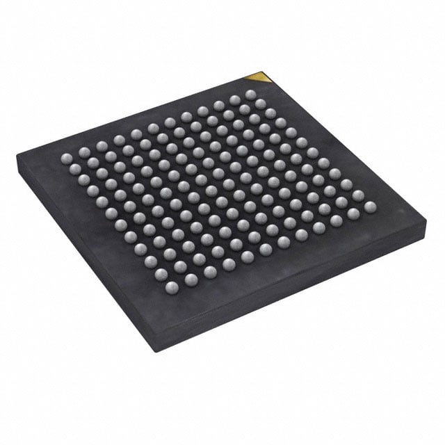
| Device Package | 144-LFBGA (12x12) | Memory Format | DRAM | Technology | SDRAM - DDR | ||
|---|---|---|---|---|---|---|---|
| Memory Size | 512 Mbit | Access Time | 700 ps | Grade | Commercial | ||
| Clock Frequency | 200 MHz | Voltage | 2.5V ~ 2.7V | Memory Type | Volatile | ||
| Operating Temperature | 0°C ~ 70°C (TA) | Write Cycle Time Word Page | 15 ns | Packaging | 144-LFBGA | ||
| Mounting Method | Volatile | Memory Interface | Parallel | Memory Organization | 16M x 32 | ||
| Moisture Sensitivity Level | 3 (168 Hours) | RoHS Compliance | ROHS Compliant | REACH Compliance | REACH Unaffected | ||
| Qualification | N/A | ECCN | EAR99 | HTS Code | 8542.32.0028 |
Overview of IS43R32160D-5BL – IC DRAM 512Mbit Parallel 144-LFBGA
The IS43R32160D-5BL is a 512‑Mbit DDR SDRAM organized as 16M × 32 with a parallel memory interface in a 144‑ball LFBGA (12×12) package. It implements double‑data‑rate architecture with a DLL and differential clock inputs to support high‑throughput burst transactions.
Designed for commercial‑temperature systems (0°C to +70°C), the device targets applications that require compact, board‑level DRAM with programmable latency, selectable burst lengths and SSTL_2‑compatible I/O for synchronized data capture.
Key Features
- DDR SDRAM Architecture Double‑data‑rate operation provides two data transfers per clock cycle with DQS strobes for edge‑aligned read and center‑aligned write timing.
- Memory Organization 512 Mbit total capacity organized as 16M × 32 with four internal banks (four banks of 128 Mb) to support concurrent operations.
- Performance Rated for a clock frequency up to 200 MHz (speed grade -5, CL = 3) and an access time of 700 ps.
- Programmable Timing and Burst Burst lengths of 2, 4 and 8, sequential and interleave burst types, and programmable CAS latency options of 2, 2.5 and 3.
- SSTL_2‑Compatible I/O and Differential Clock SSTL_2 I/O signaling with differential clock inputs (CK and CK̄) and bidirectional DQS for robust data capture.
- On‑Die Features DLL alignment of DQ/DQS with CLK, auto refresh and self refresh modes, auto precharge support and T_RAS lockout (t_RAP = t_RCD).
- Power and Timing Supply voltage range 2.5 V to 2.7 V; write cycle time (word page) of 15 ns.
- Package and Temperature 144‑LFBGA (12×12) package; commercial operating temperature range 0°C to +70°C (TA).
Typical Applications
- Commercial embedded systems — Provides board‑level DRAM capacity for general embedded memory requirements within the 0°C to +70°C temperature range.
- Compact PCB designs — 144‑LFBGA (12×12) package allows high‑density placement when 512 Mbit DDR SDRAM is required.
- System memory for synchronous data transfer — DDR architecture with DQS and differential clocking supports burst transfers and synchronized read/write operations.
Unique Advantages
- Double‑data‑rate throughput: Two data transfers per clock cycle increase effective bandwidth without increasing clock frequency.
- SSTL_2 I/O with DQS strobes: Edge‑aligned DQS for reads and center‑aligned DQS for writes improve reliable data capture at both transmitter and receiver.
- Flexible timing options: Programmable CAS latency (2, 2.5, 3) and selectable burst lengths (2/4/8) enable designers to tune performance to system requirements.
- Compact, industry‑standard package: 144‑ball LFBGA (12×12) offers a small footprint for space‑constrained boards requiring parallel DDR memory.
- Commercial temperature grading: Rated for 0°C to +70°C operation for mainstream electronic equipment.
- Robust command and refresh support: DLL, auto refresh, self refresh and auto precharge simplify memory management in continuous and low‑power modes.
Why Choose IS43R32160D-5BL?
The IS43R32160D-5BL delivers a compact 512‑Mbit DDR SDRAM solution with programmable latency, burst flexibility and SSTL_2‑compatible I/O, making it suitable for commercial embedded designs that need synchronized, high‑throughput memory in a 144‑LFBGA footprint. Its combination of DDR architecture, DLL timing alignment and differential clock inputs supports reliable burst transfers and straightforward system integration.
This device is well suited for designers seeking a standardized parallel DDR memory component with defined timing and voltage ranges (2.5 V–2.7 V) and commercial operating temperature support, enabling predictable performance and simplified BOM choices for mainstream applications.
Request a quote or submit an inquiry to obtain pricing, availability and technical support for the IS43R32160D-5BL.