IS43R83200D-6TL
| Part Description |
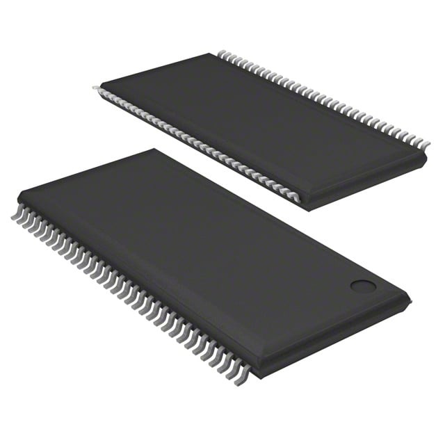
IC DRAM 256MBIT PAR 66TSOP II |
|---|---|
| Quantity | 50 Available (as of June 15, 2026) |

| Product Category | Memory |
|---|---|
| Manufacturer | Integrated Silicon Solution Inc |
| Manufacturing Status | Obsolete |
| Manufacturer Standard Lead Time | Contact Us |
| Datasheet |
Specifications & Environmental
| Device Package | 66-TSOP II | Memory Format | DRAM | Technology | SDRAM - DDR | ||
|---|---|---|---|---|---|---|---|
| Memory Size | 256 Mbit | Access Time | 700 ps | Grade | Commercial | ||
| Clock Frequency | 166 MHz | Voltage | 2.3V ~ 2.7V | Memory Type | Volatile | ||
| Operating Temperature | 0°C ~ 70°C (TA) | Write Cycle Time Word Page | 15 ns | Packaging | 66-TSSOP (0.400", 10.16mm Width) | ||
| Mounting Method | Volatile | Memory Interface | Parallel | Memory Organization | 32M x 8 | ||
| Moisture Sensitivity Level | 3 (168 Hours) | RoHS Compliance | ROHS Compliant | REACH Compliance | REACH Unaffected | ||
| Qualification | N/A | ECCN | EAR99 | HTS Code | 8542.32.0024 |
Overview of IS43R83200D-6TL – IC DRAM 256MBIT PAR 66TSOP II
The IS43R83200D-6TL is a 256‑Mbit DDR SDRAM organized as 32M × 8 bits and implemented as a parallel DRAM device in a 66‑pin TSOP‑II package. It uses double‑data‑rate architecture with a bidirectional data strobe (DQS) and an internal DLL to align data and clock edges.
This device is suited for systems that require a 256‑Mbit parallel DDR memory solution with programmable burst and CAS behavior, SSTL_2 compatible I/O, and commercial temperature operation. Key value propositions include low‑voltage operation (VDD/VDDQ ≈ 2.5 V), selectable burst length and CAS latency, and a compact 66‑TSSOP footprint for space‑constrained boards.
Key Features
- Core / Memory Architecture 256‑Mbit DDR SDRAM organized as 32M × 8 with four internal banks to support concurrent operations and continuous read/write bursts.
- DDR Data Path and Timing Double‑data‑rate transfers with bidirectional data strobe (DQS) that is edge‑aligned for READs and centre‑aligned for WRITEs; DLL aligns DQ/DQS with CK transitions. Commands are registered on the positive edge of CK.
- Performance Clock frequency up to 166 MHz (specified for the -6 speed grade) with access timing down to 700 ps and a write cycle time (word page) of 15 ns.
- Programmable Burst and Latency Burst length options of 2, 4 and 8, burst types sequential or interleave, and programmable CAS latency of 2, 2.5 and 3.
- Power and I/O VDD and VDDQ nominal 2.5 V ±0.2 V (operating supply range 2.3 V to 2.7 V) with SSTL_2 compatible I/O signaling.
- Refresh and Power Modes Supports Auto Refresh and Self Refresh modes along with Auto Precharge to manage data retention and refresh cycles.
- Package and Temperature Supplied in a 66‑TSSOP (TSOP‑II) package (0.400", 10.16 mm width) and specified for commercial temperature range 0 °C to +70 °C.
Typical Applications
- Parallel DDR memory in embedded systems Deploy where a 256‑Mbit parallel DDR SDRAM (32M × 8) is required for system memory or off‑chip data storage.
- High‑speed buffering and frame storage Use DDR double‑data‑rate transfers and DQS timing to implement read/write buffering with burst access.
- Space‑constrained board designs The 66‑TSSOP (TSOP‑II) package enables integration into compact PCB layouts.
- Commercial‑temperature embedded products Suitable for designs operating within the 0 °C to +70 °C ambient range.
Unique Advantages
- Double‑data‑rate architecture: Enables two data transfers per clock cycle, improving effective bandwidth without increasing clock rate.
- Precise data capture with DQS and DLL: Bidirectional DQS and internal DLL align data and clock edges for reliable read/write timing.
- Flexible latency and burst control: Programmable CAS latencies (2 / 2.5 / 3) and selectable burst lengths (2, 4, 8) allow tuning for system timing and throughput.
- SSTL_2 compatible I/O and low‑voltage operation: VDD/VDDQ nominal 2.5 V (2.3–2.7 V range) supports SSTL_2 signaling for compatible system interfaces.
- Concurrent bank operation: Four internal banks allow overlapping commands and improved command throughput for burst sequences.
- Compact package footprint: 66‑TSSOP (TSOP‑II) package provides a smaller PCB area compared with larger BGAs for suitable applications.
Why Choose IS43R83200D-6TL?
The IS43R83200D-6TL delivers a compact, standard‑form DDR SDRAM solution with explicit timing control, SSTL_2 compatible I/O, and programmable burst and latency options. Its 32M × 8 organization and four‑bank architecture support bursty and concurrent memory operations while fitting into 66‑TSSOP board layouts.
This device is appropriate for designers needing a 256‑Mbit parallel DDR memory component within the commercial temperature range, and for applications that require configurable burst behavior, reliable DQS timing, and low‑voltage SSTL_2 signaling. It is manufactured by Integrated Silicon Solution, Inc.
Request a quote or submit an inquiry to receive pricing and availability information for the IS43R83200D-6TL.