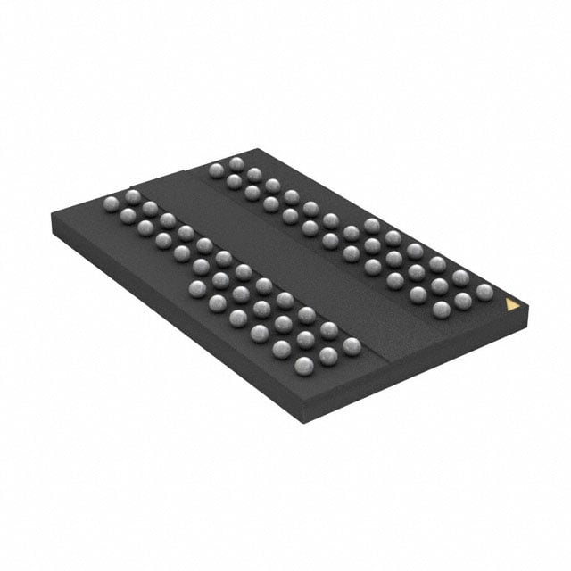
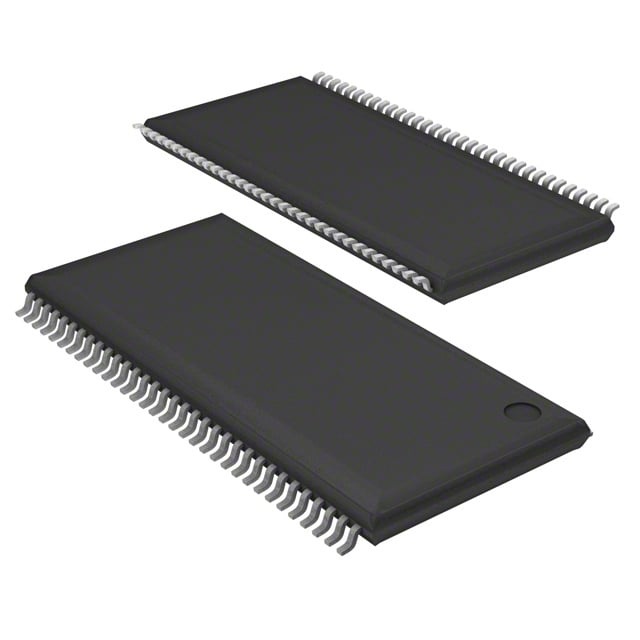
IS43R86400D-5TLI
| Part Description |
IC DRAM 512MBIT PAR 66TSOP II |
|---|---|
| Quantity | 188 Available (as of June 15, 2026) |

| Product Category | Memory |
|---|---|
| Manufacturer | Integrated Silicon Solution Inc |
| Manufacturing Status | Obsolete |
| Manufacturer Standard Lead Time | Contact Us |
| Datasheet |
Specifications & Environmental
| Device Package | 66-TSOP II | Memory Format | DRAM | Technology | SDRAM - DDR | ||
|---|---|---|---|---|---|---|---|
| Memory Size | 512 Mbit | Access Time | 700 ps | Grade | Industrial | ||
| Clock Frequency | 200 MHz | Voltage | 2.5V ~ 2.7V | Memory Type | Volatile | ||
| Operating Temperature | -40°C ~ 85°C (TA) | Write Cycle Time Word Page | 15 ns | Packaging | 66-TSSOP (0.400", 10.16mm Width) | ||
| Mounting Method | Volatile | Memory Interface | Parallel | Memory Organization | 64M x 8 | ||
| Moisture Sensitivity Level | 3 (168 Hours) | RoHS Compliance | ROHS Compliant | REACH Compliance | REACH Unaffected | ||
| Qualification | N/A | ECCN | EAR99 | HTS Code | 8542.32.0028 |
Overview of IS43R86400D-5TLI – 512Mbit DDR SDRAM, 66-TSOP II
The IS43R86400D-5TLI is a 512‑Mbit DDR SDRAM organized as 64M × 8 bits in a 66‑pin TSOP‑II package. It implements a double‑data‑rate architecture with internal banking and programmable burst/CAS behavior to support high‑speed parallel memory subsystems.
Designed for systems requiring pipelined read/write bursts and SSTL_2 compatible I/O, this device targets applications that need controlled timing, low‑voltage DDR operation and an industrial temperature range.
Key Features
- Memory Core — 512 Mbit DRAM organized as 64M × 8 with four internal banks for concurrent operations and pipelined access.
- DDR Performance — Double‑data‑rate architecture with two data transfers per clock cycle; Fck up to 200 MHz (speed grade -5 at CL=3).
- Programmable Burst and Latency — Burst lengths of 2, 4 and 8 with sequential and interleave modes; programmable CAS latency options of 2, 2.5 and 3.
- Data Timing and Capture — Bidirectional data strobe (DQS) transmitted/received with data; DQS edge‑aligned for READs and center‑aligned for WRITEs; data and mask referenced to both edges of DQS.
- Clocking and DLL — Differential clock inputs (CK and CK̄) with on‑die DLL to align DQ/DQS transitions to clock edges; commands are registered on positive CK edges.
- I/O Standard — SSTL_2 compatible I/O signaling with separate VDD and VDDQ supply options (2.5 V ±0.2 V or 2.6 V ±0.1 V depending on grade); operating supply range 2.5 V to 2.7 V.
- Refresh and Power Modes — Auto Refresh, Self Refresh and Auto Precharge supported for standard DRAM power management and retention.
- Timing and Throughput — Specified access timing such as 700 ps access time and a word page write cycle time of 15 ns to support high throughput burst operations.
- Package and Temperature — 66‑pin TSOP‑II (66‑TSSOP, 0.400" / 10.16 mm width) package; operating temperature range −40 °C to +85 °C (TA).
Typical Applications
- Embedded memory subsystems — Provides 512 Mbit parallel DDR storage for embedded designs requiring pipelined read/write burst transfers.
- High‑speed buffering — Used where burstable DDR access and low‑voltage SSTL_2 I/O are needed for transient data buffering.
- Industrial electronics — Operates across an industrial temperature range (−40 °C to +85 °C) for systems deployed in varied environments.
Unique Advantages
- High throughput DDR architecture: Double‑data‑rate operation and programmable burst lengths deliver increased data transfers per clock without extra clock rate.
- Flexible timing control: Programmable CAS latencies (2 / 2.5 / 3) and burst modes allow tuning for system timing and latency requirements.
- Robust data capture: Bidirectional DQS with edge/center alignment and DLL alignment ensures precise data timing for read and write operations.
- Industrial temperature support: Specified operation from −40 °C to +85 °C for deployment in temperature‑sensitive applications.
- Compact board footprint: Available in a 66‑TSOP II package (0.400" / 10.16 mm width) suitable for space‑constrained PCB designs.
Why Choose IC DRAM 512MBIT PAR 66TSOP II?
The IS43R86400D-5TLI balances DDR performance, configurable timing and a compact TSOP‑II package for designs that require 512 Mbit of parallel DDR SDRAM with controlled I/O and refresh features. Its SSTL_2 compatible I/O, DLL clock alignment and programmable burst/CAS options make it suitable for systems that need precise timing and sustained burst throughput.
Manufactured by Integrated Silicon Solution Inc., this device is intended for engineers and procurement teams seeking a proven 64M × 8 DDR SDRAM device with industrial temperature capability and a small package footprint.
Request a quote or submit an inquiry for the IS43R86400D-5TLI to evaluate availability and pricing for your design needs.