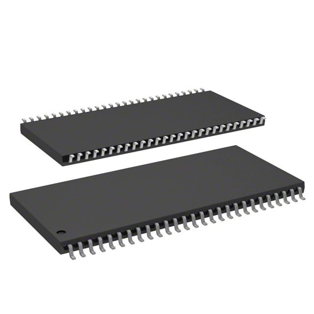
IS45S16160D-7TLA1
| Part Description |
IC DRAM 256MBIT PAR 54TSOP II |
|---|---|
| Quantity | 961 Available (as of June 15, 2026) |

| Product Category | Memory |
|---|---|
| Manufacturer | Integrated Silicon Solution Inc |
| Manufacturing Status | Obsolete |
| Manufacturer Standard Lead Time | Contact Us |
| Datasheet |
Specifications & Environmental
| Device Package | 54-TSOP II | Memory Format | DRAM | Technology | SDRAM | ||
|---|---|---|---|---|---|---|---|
| Memory Size | 256 Mbit | Access Time | 5.4 ns | Grade | Industrial | ||
| Clock Frequency | 143 MHz | Voltage | 3V ~ 3.6V | Memory Type | Volatile | ||
| Operating Temperature | -40°C ~ 85°C (TA) | Write Cycle Time Word Page | N/A | Packaging | 54-TSOP (0.400", 10.16mm Width) | ||
| Mounting Method | Volatile | Memory Interface | Parallel | Memory Organization | 16M x 16 | ||
| Moisture Sensitivity Level | 3 (168 Hours) | RoHS Compliance | ROHS3 Compliant | REACH Compliance | REACH Unaffected | ||
| Qualification | N/A | ECCN | EAR99 | HTS Code | 8542.32.0028 |
Overview of IS45S16160D-7TLA1 – IC DRAM 256MBIT PAR 54TSOP II
The IS45S16160D-7TLA1 is a 256‑Mbit synchronous DRAM organized as 16M × 16 with a parallel memory interface. It uses a pipeline architecture with all signals referenced to the rising edge of the clock to enable high-speed data transfer.
Designed for boards requiring a 54‑pin TSOP‑II footprint and a single 3.3V power rail, this device provides programmable burst and latency options, LVTTL signaling, and refresh modes to support a range of synchronous memory needs in system-level designs.
Key Features
- Core and Architecture Pipeline, fully synchronous design; all inputs and outputs referenced to the positive clock edge and internal bank architecture for hiding row access/precharge.
- Memory Organization 256 Mbit SDRAM organized as 16M × 16 with four internal banks.
- Performance Clock frequency support to 143 MHz (device option); access time 5.4 ns (CAS latency = 3).
- Burst and Access Modes Programmable burst lengths (1, 2, 4, 8, full page), programmable burst sequence (sequential/interleave), burst read/write and burst read/single write operations, and burst termination commands.
- Refresh and Self-Refresh Auto Refresh (CBR) and Self Refresh supported; 8K refresh cycles with options for 16 ms (A2 grade) or 64 ms (commercial/industrial/A1 grade).
- Interface and Signaling Parallel memory interface with LVTTL signaling and random column address every clock cycle.
- Power Single power supply: 3.3V ±0.3V (3.0–3.6V supply range).
- Package and Temperature 54‑pin TSOP‑II package (0.400", 10.16 mm width); operating temperature range −40°C to +85°C (TA).
Typical Applications
- High-speed data buffering — Use as synchronous DRAM in designs that require pipeline architecture and high-speed data transfer.
- System memory for parallel interfaces — 16M × 16 organization and LVTTL signaling support parallel system-memory implementations with per-clock random column access.
- Board-level memory expansion — Standard 54‑pin TSOP‑II footprint and single 3.3V supply make this device suitable for PCB memory expansion where a compact TSOP‑II package is required.
Unique Advantages
- High-speed synchronous operation: 143 MHz clock support and pipeline architecture enable clock-referenced, high-throughput data transfers.
- Low-latency access: 5.4 ns access time at CAS latency = 3 provides fast read responsiveness for synchronous workloads.
- Flexible burst control: Programmable burst lengths and sequencing allow tuning for different access patterns and throughput requirements.
- Robust refresh options: Auto and self-refresh modes with selectable refresh timing to match device grade and system power profiles.
- Simplified power rail: Single 3.3V supply (3.0–3.6V) reduces board power-rail complexity.
- Compact, standard package: 54‑pin TSOP‑II (10.16 mm width) supports dense PCB layouts using a common footprint.
Why Choose IC DRAM 256MBIT PAR 54TSOP II?
The IS45S16160D-7TLA1 positions itself as a practical 256‑Mbit SDRAM option for designs that need synchronous, parallel memory with programmable burst behavior and selectable CAS latency. Its pipeline architecture, LVTTL interface, and refresh/self-refresh capabilities make it suitable for system-level memory implementations requiring predictable timing and high data throughput.
Packaged in a 54‑pin TSOP‑II and operating from a single 3.3V rail across −40°C to +85°C, the device offers a balance of performance, compactness, and thermal range for designers specifying board-level DRAM from Integrated Silicon Solution, Inc.
Request a quote or submit a pricing and availability inquiry for IS45S16160D-7TLA1 to receive detailed ordering information and lead-time options.