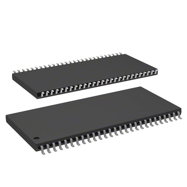
IS45S16160D-7TLA2
| Part Description |
IC DRAM 256MBIT PAR 54TSOP II |
|---|---|
| Quantity | 411 Available (as of June 15, 2026) |

| Product Category | Memory |
|---|---|
| Manufacturer | Integrated Silicon Solution Inc |
| Manufacturing Status | Obsolete |
| Manufacturer Standard Lead Time | Contact Us |
| Datasheet |
Specifications & Environmental
| Device Package | 54-TSOP II | Memory Format | DRAM | Technology | SDRAM | ||
|---|---|---|---|---|---|---|---|
| Memory Size | 256 Mbit | Access Time | 5.4 ns | Grade | Automotive | ||
| Clock Frequency | 143 MHz | Voltage | 3V ~ 3.6V | Memory Type | Volatile | ||
| Operating Temperature | -40°C ~ 105°C (TA) | Write Cycle Time Word Page | N/A | Packaging | 54-TSOP (0.400", 10.16mm Width) | ||
| Mounting Method | Volatile | Memory Interface | Parallel | Memory Organization | 16M x 16 | ||
| Moisture Sensitivity Level | 3 (168 Hours) | RoHS Compliance | ROHS3 Compliant | REACH Compliance | REACH Unaffected | ||
| Qualification | N/A | ECCN | EAR99 | HTS Code | 8542.32.0028 |
Overview of IS45S16160D-7TLA2 – 256Mbit Synchronous DRAM, 54‑TSOP II
The IS45S16160D-7TLA2 is a 256‑Mbit synchronous DRAM (SDRAM) organized as 16M × 16 with internal bank architecture. It implements a pipelined, fully synchronous design where all inputs and outputs are referenced to the rising edge of the clock to support high‑speed, clocked memory access.
This device targets applications requiring parallel SDRAM with programmable burst and latency options, offering configurable CAS latency, burst sequencing and on‑chip refresh management to simplify system memory timing and control.
Key Features
- Memory Architecture — 256 Mbit SDRAM organized as 16M × 16 with 4 internal banks to support efficient row/column access and bank‑level precharge hiding.
- Clocked Performance — Supports clock frequencies up to 143 MHz (‑7 speed grade) with an access time from clock of 5.4 ns at CAS latency = 3.
- Programmable Burst and Latency — Programmable burst lengths (1, 2, 4, 8, full page), sequential or interleaved burst sequences, and selectable CAS latency (2 or 3 clocks) for flexible throughput tuning.
- Refresh and Retention — Auto Refresh and Self Refresh support with 8K refresh cycles; refresh intervals provided for A2 grade (8K/16 ms) and commercial/industrial/A1 grade (8K/64 ms).
- Supply and I/O — Single power supply: 3.3 V ±0.3 V (3.0 V–3.6 V); LVTTL interface for command and control signals.
- Parallel SDRAM Interface — Standard parallel DRAM interface suitable for memory subsystems requiring synchronous, clock‑referenced data transfers.
- Package and Mounting — Available in a 54‑pin TSOP‑II package (0.400" / 10.16 mm width) for board‑level mounting.
- Operating Temperature — Rated for −40°C to +105°C (TA) for extended temperature applications.
Typical Applications
- High‑speed system memory — Provides synchronous, pipelined DRAM storage where clock‑referenced bursts and programmable CAS latency are required.
- Streaming and buffer memory — Programmable burst lengths and burst sequencing support burst read/write operations for data buffering and streaming tasks.
- Embedded memory subsystems — Parallel SDRAM interface and standard TSOP‑II package simplify integration into board‑level memory arrays and controllers.
Unique Advantages
- Flexible performance scaling — Selectable CAS latency (2 or 3) and multiple burst length options enable tuning for latency or throughput depending on system needs.
- Clock‑synchronous pipeline — All signals referenced to the rising edge of the clock and pipeline architecture support predictable timing and high‑speed transfers.
- On‑chip refresh management — Auto Refresh and Self Refresh modes with documented refresh intervals reduce external refresh control complexity.
- Wide operating voltage range — 3.0 V–3.6 V supply tolerance (3.3 V ±0.3 V) helps compatibility with common 3.3 V system rails.
- Extended temperature capability — Rated to −40°C to +105°C (TA) for deployments in environments requiring extended temperature range.
- Compact board footprint — 54‑pin TSOP‑II package provides a common surface‑mount option for compact memory designs.
Why Choose IS45S16160D-7TLA2?
The IS45S16160D-7TLA2 combines a pipelined, fully synchronous SDRAM architecture with programmable latency and burst controls to deliver predictable, high‑speed parallel memory performance. Its on‑chip refresh modes, LVTTL interface and standard TSOP‑II package make it a practical option for designers needing configurable DRAM capacity and timing in board‑level memory subsystems.
This device is suitable for designs that require scalable memory performance with clear timing control and extended operating temperature support, providing a straightforward path for integrating 256 Mbit SDRAM where parallel, clocked access and burst operations are required.
Request a quote or contact sales to discuss availability, lead times and volume pricing for the IS45S16160D-7TLA2.