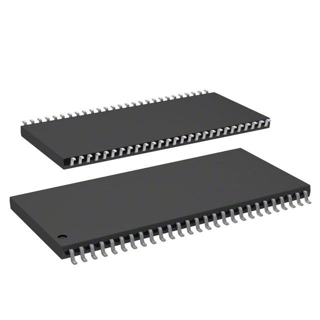
IS45S16320D-7CTLA1-TR
| Part Description |
IC DRAM 512MBIT PAR 54TSOP II |
|---|---|
| Quantity | 830 Available (as of June 15, 2026) |

| Product Category | Memory |
|---|---|
| Manufacturer | Integrated Silicon Solution Inc |
| Manufacturing Status | Obsolete |
| Manufacturer Standard Lead Time | Contact Us |
| Datasheet |
Specifications & Environmental
| Device Package | 54-TSOP II | Memory Format | DRAM | Technology | SDRAM | ||
|---|---|---|---|---|---|---|---|
| Memory Size | 512 Mbit | Access Time | 5.4 ns | Grade | Industrial | ||
| Clock Frequency | 143 MHz | Voltage | 3V ~ 3.6V | Memory Type | Volatile | ||
| Operating Temperature | -40°C ~ 85°C (TA) | Write Cycle Time Word Page | N/A | Packaging | 54-TSOP (0.400", 10.16mm Width) | ||
| Mounting Method | Volatile | Memory Interface | Parallel | Memory Organization | 32M x 16 | ||
| Moisture Sensitivity Level | 3 (168 Hours) | RoHS Compliance | ROHS3 Compliant | REACH Compliance | REACH Unaffected | ||
| Qualification | N/A | ECCN | EAR99 | HTS Code | 8542.32.0032 |
Overview of IS45S16320D-7CTLA1-TR – IC DRAM 512MBIT PAR 54TSOP II
The IS45S16320D-7CTLA1-TR is a 512 Mbit synchronous DRAM organized as 32M × 16 and implemented in a 54-pin TSOP-II package. It uses a fully synchronous pipeline architecture with a parallel memory interface designed for high-speed data transfer in synchronous systems.
Key value comes from its programmable burst operation, internal bank structure for hidden row access/precharge, and timing options tuned for a 143 MHz clock (–7 timing), making it suitable for designs that require predictable, low-latency SDRAM behavior within a compact TSOP footprint.
Key Features
- Memory Type & Capacity — 512 Mbit SDRAM organized as 32M × 16, providing a wide data path for parallel synchronous operations.
- Clocking & Performance — Supports −7 timing with a clock frequency of 143 MHz and an access time from clock of 5.4 ns (CAS latency options available), delivering deterministic synchronous read/write timing.
- Programmable Burst & CAS — Programmable burst lengths (1, 2, 4, 8, full page) and selectable burst sequence (sequential/interleave); programmable CAS latency (2 or 3 clocks) for flexible trade-offs between throughput and latency.
- Banking & Refresh — Internal bank architecture to hide row access/precharge and support for Auto Refresh and Self Refresh modes; 8K refresh cycles per 64 ms.
- Interface & Signaling — LVTTL-compatible parallel interface enabling random column access every clock cycle and standard synchronous control signaling referenced to the positive clock edge.
- Power — Supply voltage specified at 3.0 V to 3.6 V for the device variant, supporting common 3.3 V system rails.
- Package & Temperature — 54-pin TSOP-II (0.400", 10.16 mm width) package; operating temperature range −40 °C to +85 °C (TA).
Typical Applications
- Synchronous system memory — High-speed SDRAM for systems that require pipelined, clock-synchronous main or buffer memory with parallel access.
- Data buffering and burst transfer — Useful where programmable burst lengths and low-latency CAS options improve throughput for burst read/write operations.
- Compact board-level memory expansion — 54-TSOP-II package provides a space-efficient footprint for designs requiring 512 Mbit of parallel SDRAM.
Unique Advantages
- Deterministic synchronous operation: Fully synchronous design with all signals referenced to the positive clock edge supports predictable timing and system integration.
- Flexible performance tuning: Programmable CAS latency and burst length/sequence allow optimization between latency and sustained throughput.
- High-frequency support: −7 timing rated for 143 MHz clock operation with 5.4 ns access time from clock, suitable for higher-speed synchronous designs.
- Robust refresh and low-power modes: Auto Refresh and Self Refresh support with standard 8K refresh cycles per 64 ms helps maintain data integrity across operating conditions.
- Compact package: 54-pin TSOP-II provides a narrow, board-friendly package option for space-constrained layouts.
- Wide operating voltage and temperature range: 3.0 V–3.6 V supply range and −40 °C to +85 °C operating temperature support common 3.3 V systems and extended temperature applications.
Why Choose IS45S16320D-7CTLA1-TR?
The IS45S16320D-7CTLA1-TR combines a compact 54-TSOP-II package with a fully synchronous SDRAM architecture and flexible timing options, making it a practical choice for designs that need 512 Mbit of parallel memory with predictable, low-latency behavior. Its programmable burst features, internal banking, and standard refresh mechanisms allow engineers to tune memory behavior for a range of synchronous data-transfer requirements.
This device is well suited to system designs that require a reliable, board-level SDRAM component with 143 MHz (−7) timing capability, LVTTL-compatible parallel interface, and an industrial-temperature range for extended deployments.
Request a quote or submit an inquiry for IS45S16320D-7CTLA1-TR to check availability, pricing, and lead times for your next design.