IS45S16320D-7TLA1-TR
| Part Description |
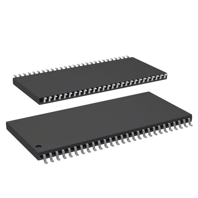
IC DRAM 512MBIT PAR 54TSOP II |
|---|---|
| Quantity | 1,091 Available (as of June 15, 2026) |

| Product Category | Memory |
|---|---|
| Manufacturer | Integrated Silicon Solution Inc |
| Manufacturing Status | Obsolete |
| Manufacturer Standard Lead Time | Contact Us |
| Datasheet |
Specifications & Environmental
| Device Package | 54-TSOP II | Memory Format | DRAM | Technology | SDRAM | ||
|---|---|---|---|---|---|---|---|
| Memory Size | 512 Mbit | Access Time | 5.4 ns | Grade | Industrial | ||
| Clock Frequency | 143 MHz | Voltage | 3V ~ 3.6V | Memory Type | Volatile | ||
| Operating Temperature | -40°C ~ 85°C (TA) | Write Cycle Time Word Page | N/A | Packaging | 54-TSOP (0.400", 10.16mm Width) | ||
| Mounting Method | Volatile | Memory Interface | Parallel | Memory Organization | 32M x 16 | ||
| Moisture Sensitivity Level | 3 (168 Hours) | RoHS Compliance | ROHS3 Compliant | REACH Compliance | REACH Unaffected | ||
| Qualification | N/A | ECCN | EAR99 | HTS Code | 8542.32.0032 |
Overview of IS45S16320D-7TLA1-TR – IC DRAM 512Mbit PAR 54TSOP II
The IS45S16320D-7TLA1-TR is a 512Mbit synchronous DRAM organized as 32M × 16 with a parallel LVTTL interface and pipeline architecture. It delivers synchronous, high-speed data transfer with programmable burst lengths and internal bank management to optimize row access and precharge.
Designed for systems that require medium-density, high-throughput volatile memory, this device combines a compact 54-pin TSOP-II package, 3.0–3.6 V supply range, and an extended operating temperature rating to support a range of embedded and industrial memory subsystem designs.
Key Features
- Memory Core 512 Mbit SDRAM organized as 32M × 16 with internal bank architecture for hidden row access/precharge.
- Performance & Timing Clock frequency supported at 143 MHz for the -7 timing grade with access time from clock as low as 5.4 ns (CAS latency = 3).
- Burst & Latency Programmable burst lengths (1, 2, 4, 8, full page) and selectable burst sequence (sequential/interleave); programmable CAS latency options (2 or 3 clocks).
- Refresh & Self-maintenance Auto Refresh (CBR) and Self Refresh supported with 8K refresh cycles per 64 ms (standard refresh modes provided).
- Power & Voltage Operates from 3.0 V to 3.6 V (VDD/VDDQ specified), supporting standard 3.3 V system environments.
- Interface Parallel LVTTL-compatible interface with random column address capability every clock cycle and burst read/write operations.
- Package & Mounting Available in a 54-pin TSOP-II (0.400", 10.16 mm width) package for compact board-level integration.
- Operating Temperature Industrial temperature range: −40°C to +85°C (TA).
Typical Applications
- Memory subsystems and buffers Use where a 512 Mbit synchronous DRAM with 32M × 16 organization and programmable burst support is required for intermediate storage and buffering.
- Embedded systems with parallel DRAM interface Suited to designs that require a parallel LVTTL SDRAM interface and predictable, synchronous timing behavior.
- Industrial equipment Applicable for industrial designs needing extended temperature support (−40°C to +85°C) and stable 3.0–3.6 V supply operation.
- High-throughput data applications Systems that benefit from pipeline architecture, internal bank management and programmable burst modes to sustain frequent, high-speed memory accesses.
Unique Advantages
- Deterministic synchronous operation: The device references all inputs and outputs to the positive clock edge, enabling predictable timing and pipeline data flow.
- Flexible timing grades: Available timing grades include options up to 143 MHz for the -7 variant, with CAS latency options of 2 or 3 clocks to match system timing requirements.
- Compact TSOP-II footprint: 54-pin TSOP-II package provides a space-efficient solution for board designs requiring 16-bit parallel SDRAM.
- On-chip refresh and self-refresh: Auto Refresh (CBR) and Self Refresh features simplify external refresh control and support low-maintenance memory operation.
- Wide supply tolerance: 3.0–3.6 V supply range gives compatibility with standard 3.3 V systems while allowing some supply variation tolerance.
- Industrial temperature rating: Specified for −40°C to +85°C to support deployments in temperature-challenging environments.
Why Choose IS45S16320D-7TLA1-TR?
The IS45S16320D-7TLA1-TR is positioned for designs that need a reliable 512 Mbit synchronous DRAM with predictable, high-speed operation and flexible burst/latency control. Its pipeline architecture, internal bank management, and programmable operating modes provide designers with control over throughput and timing behavior.
This device is well suited to embedded and industrial memory subsystems that require a compact 54-pin TSOP-II package, a standard 3.0–3.6 V supply window, and an extended −40°C to +85°C operating range. Engineers seeking a straightforward, synchronous parallel DRAM building block for buffering, high-throughput access, and compact board layouts will find the IS45S16320D-7TLA1-TR aligned to those needs.
Request a quote or submit an RFQ to obtain pricing, availability, and lead-time information for the IS45S16320D-7TLA1-TR.