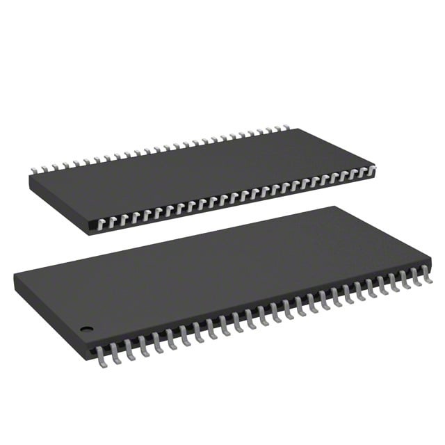
IS45S16320D-7TLA2-TR
| Part Description |
IC DRAM 512MBIT PAR 54TSOP II |
|---|---|
| Quantity | 955 Available (as of June 15, 2026) |

| Product Category | DRAM Memory |
|---|---|
| Manufacturer | Integrated Silicon Solution Inc |
| Manufacturing Status | Obsolete |
| Manufacturer Standard Lead Time | Contact Us |
| Datasheet |
Specifications & Environmental
| Device Package | 54-TSOP II | Memory Format | DRAM | Technology | SDRAM | ||
|---|---|---|---|---|---|---|---|
| Memory Size | 512 Mbit | Access Time | 5.4 ns | Grade | Automotive | ||
| Clock Frequency | 143 MHz | Voltage | 3V ~ 3.6V | Memory Type | Volatile | ||
| Operating Temperature | -40°C ~ 105°C (TA) | Write Cycle Time Word Page | N/A | Packaging | 54-TSOP (0.400", 10.16mm Width) | ||
| Mounting Method | Volatile | Memory Interface | Parallel | Memory Organization | 32M x 16 | ||
| Moisture Sensitivity Level | 3 (168 Hours) | RoHS Compliance | ROHS3 Compliant | REACH Compliance | REACH Unaffected | ||
| Qualification | N/A | ECCN | EAR99 | HTS Code | 8542.32.0032 |
Overview of IS45S16320D-7TLA2-TR – IC DRAM 512MBIT PAR 54TSOP II
The IS45S16320D-7TLA2-TR is a 512Mbit synchronous DRAM (SDRAM) organized as 32M × 16 with a parallel memory interface. It implements a fully synchronous pipeline architecture with internal bank management to support high-throughput memory operations in systems that require discrete SDRAM devices.
Targeted for applications requiring a compact 54-pin TSOP-II footprint, this device delivers a 143 MHz clock frequency and a 5.4 ns access time (CAS latency depending on configuration), while operating from a 3.0 V to 3.6 V supply and across a broad temperature range.
Key Features
- Core Memory Architecture 512 Mbit SDRAM organized as 32M × 16 with internal banking to hide row access and precharge operations.
- Synchronous, High-Speed Operation Fully synchronous design with signals referenced to the rising clock edge; specified for a 143 MHz clock frequency (–7 speed grade) and 5.4 ns access time.
- Flexible Burst and Latency Options Programmable burst lengths (1, 2, 4, 8, full page) and burst sequence (sequential/interleave); programmable CAS latency options are supported.
- Refresh and Self-Refresh Supports Auto Refresh (CBR), Self Refresh, and 8K refresh cycles per 64 ms to maintain data integrity.
- Interface Parallel memory interface with LVTTL-compatible signaling for command and control.
- Power Rated for VDD/VDDQ operation from 3.0 V to 3.6 V.
- Package 54-pin TSOP-II (0.400", 10.16 mm width) package suitable for compact board layouts; supplier device package listed as 54-TSOP II.
- Operating Temperature Specified operating ambient temperature range of −40°C to +105°C (TA).
Typical Applications
- Embedded memory subsystems Use as discrete SDRAM for systems requiring a parallel synchronous memory interface and compact TSOP-II packaging.
- Buffering and data staging Suitable for applications that need burst-capable read/write operations and predictable CAS latency for data buffering.
- Industrial electronics Applicable in designs where a wide operating temperature range and a 3.0–3.6 V supply are required.
Unique Advantages
- Predictable timing performance: 143 MHz clock speed and 5.4 ns access time (–7 grade) provide defined timing for system memory design and latency budgeting.
- Flexible data transfer modes: Programmable burst lengths and sequence options enable optimization for sequential or random access patterns.
- Robust refresh management: Auto and self-refresh support with 8K refresh cycles per 64 ms simplify retention control in active and low-power states.
- Wide supply compatibility: 3.0 V to 3.6 V VDD/VDDQ range supports common 3.3 V system rails.
- Compact board footprint: 54-pin TSOP-II package (10.16 mm width) enables memory integration on space-constrained PCBs.
- Broad ambient range: Specified operation from −40°C to +105°C (TA) addresses applications with elevated environmental requirements.
Why Choose IC DRAM 512MBIT PAR 54TSOP II?
The IS45S16320D-7TLA2-TR provides a synchronous, parallel 512 Mbit memory solution with defined timing (143 MHz, 5.4 ns) and flexible burst/latency configuration. Its combination of internal bank architecture, standard LVTTL interface, and comprehensive refresh features makes it suitable for designs that require predictable SDRAM behavior in a compact TSOP-II package.
This device is well suited to engineers specifying discrete SDRAM for embedded and industrial-grade systems that operate from 3.0–3.6 V and across a broad ambient temperature range. Its programmable transfer modes and refresh capabilities support a range of memory access patterns while simplifying system-level memory management.
Request a quote or submit a quotation request to obtain pricing and availability for the IS45S16320D-7TLA2-TR.