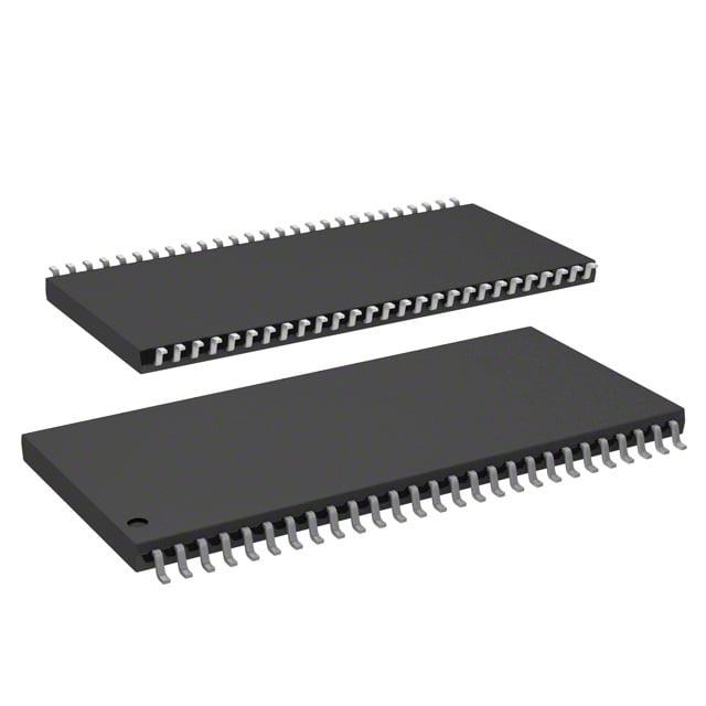
IS45S16320D-7CTLA2
| Part Description |
IC DRAM 512MBIT PAR 54TSOP II |
|---|---|
| Quantity | 486 Available (as of June 10, 2026) |

| Product Category | Memory |
|---|---|
| Manufacturer | Integrated Silicon Solution Inc |
| Manufacturing Status | Obsolete |
| Manufacturer Standard Lead Time | Contact Us |
| Datasheet |
Specifications & Environmental
| Device Package | 54-TSOP II | Memory Format | DRAM | Technology | SDRAM | ||
|---|---|---|---|---|---|---|---|
| Memory Size | 512 Mbit | Access Time | 5.4 ns | Grade | Automotive | ||
| Clock Frequency | 143 MHz | Voltage | 3V ~ 3.6V | Memory Type | Volatile | ||
| Operating Temperature | -40°C ~ 105°C (TA) | Write Cycle Time Word Page | N/A | Packaging | 54-TSOP (0.400", 10.16mm Width) | ||
| Mounting Method | Volatile | Memory Interface | Parallel | Memory Organization | 32M x 16 | ||
| Moisture Sensitivity Level | 3 (168 Hours) | RoHS Compliance | ROHS3 Compliant | REACH Compliance | REACH Unaffected | ||
| Qualification | N/A | ECCN | EAR99 | HTS Code | 8542.32.0032 |
Overview of IS45S16320D-7CTLA2 – IC DRAM 512MBIT PAR 54TSOP II
The IS45S16320D-7CTLA2 is a 512 Mbit synchronous DRAM organized as 32M × 16, delivered in a 54-pin TSOP-II package. It implements a fully synchronous pipeline architecture with internal bank management and a parallel LVTTL interface to support high-speed, clock-referenced memory operations.
Designed for applications that require deterministic burst transfers and refresh management, this device offers programmable burst length and sequence, selectable CAS latency, and power options suited to 3.0–3.6 V systems, with an extended operating temperature range of −40°C to +105°C (TA).
Key Features
- Memory Organization — 512 Mbit total capacity arranged as 32M × 16, providing a wide data path for parallel memory systems.
- Fully Synchronous SDRAM — All inputs and outputs are referenced to the positive clock edge; device implements pipeline architecture and internal bank structure to hide row access/precharge.
- Performance — Supported clock frequency for the -7 grade is 143 MHz with an access time from clock as low as 5.4 ns (CAS latency options 2 or 3).
- Flexible Burst Operation — Programmable burst lengths (1, 2, 4, 8, full page) and burst sequence (sequential/interleave) for efficient block transfers.
- Refresh and Low-Power Modes — Auto Refresh (CBR), Self Refresh, and 8K refresh cycles every 64 ms to maintain data integrity across operating conditions.
- Interface and Signaling — Parallel LVTTL interface compatible with standard synchronous DRAM control signals and programmable CAS latency (2, 3 clocks).
- Power Supply — Operates from a 3.0 V to 3.6 V supply range (VDD / VDDQ as specified for the S device family).
- Package and Temperature — 54-pin TSOP-II package (0.400", 10.16 mm width) with an operating temperature range of −40°C to +105°C (TA).
Typical Applications
- High-speed memory subsystems — Used where clock-referenced burst transfers and low access latency are required for parallel data buffering.
- Systems requiring programmable burst control — Suitable for designs that leverage selectable burst length and sequence to optimize block read/write behavior.
- Environments with extended temperature needs — Applicable to equipment that must operate reliably across −40°C to +105°C ambient conditions.
- Designs needing deterministic CAS timing — Deployable in architectures that require selectable CAS latency (2 or 3) to meet timing margins.
Unique Advantages
- Deterministic synchronous operation: Fully synchronous design with clock-referenced I/O ensures predictable timing for high-speed systems.
- Flexible burst control: Programmable burst lengths and sequence let designers tune throughput and latency for specific data transfer patterns.
- Internal bank architecture: Banked memory and pipeline access hide row precharge/activation, improving effective throughput for interleaved operations.
- Wide operating voltage window: Compatibility with 3.0–3.6 V supplies accommodates a range of system power rails.
- Extended temperature capability: Specified operation from −40°C to +105°C (TA) supports deployment in thermally challenging environments.
Why Choose IC DRAM 512MBIT PAR 54TSOP II?
The IS45S16320D-7CTLA2 positions itself as a reliable 512 Mbit SDRAM option when synchronous, parallel memory with programmable burst behavior and selectable CAS latency is required. Its 32M × 16 organization, pipeline architecture, and internal bank management provide predictable performance for systems that depend on high-throughput, clocked memory accesses.
This device is well suited to designs that need a compact 54-pin TSOP-II package, a 3.0–3.6 V supply domain, and extended ambient operation. It delivers measurable design flexibility through configurable burst modes and refresh options while maintaining verifiable timing characteristics such as a 143 MHz clock grade and 5.4 ns access time from clock.
Request a quote or submit an inquiry to receive pricing, availability, and support information for IS45S16320D-7CTLA2.