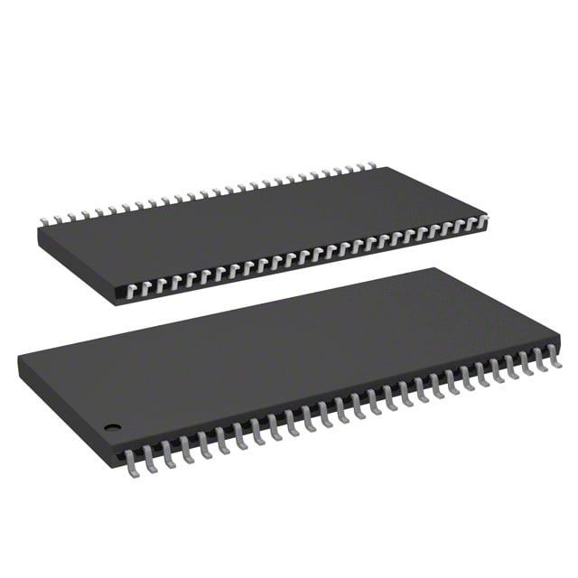
IS45S16320D-7CTLA1
| Part Description |
IC DRAM 512MBIT PAR 54TSOP II |
|---|---|
| Quantity | 859 Available (as of June 15, 2026) |

| Product Category | DRAM Memory |
|---|---|
| Manufacturer | Integrated Silicon Solution Inc |
| Manufacturing Status | Obsolete |
| Manufacturer Standard Lead Time | Contact Us |
| Datasheet |
Specifications & Environmental
| Device Package | 54-TSOP II | Memory Format | DRAM | Technology | SDRAM | ||
|---|---|---|---|---|---|---|---|
| Memory Size | 512 Mbit | Access Time | 5.4 ns | Grade | Industrial | ||
| Clock Frequency | 143 MHz | Voltage | 3V ~ 3.6V | Memory Type | Volatile | ||
| Operating Temperature | -40°C ~ 85°C (TA) | Write Cycle Time Word Page | N/A | Packaging | 54-TSOP (0.400", 10.16mm Width) | ||
| Mounting Method | Volatile | Memory Interface | Parallel | Memory Organization | 32M x 16 | ||
| Moisture Sensitivity Level | 3 (168 Hours) | RoHS Compliance | ROHS3 Compliant | REACH Compliance | REACH Unaffected | ||
| Qualification | N/A | ECCN | EAR99 | HTS Code | 8542.32.0032 |
Overview of IS45S16320D-7CTLA1 – 512Mbit SDRAM, 54-TSOP II
The IS45S16320D-7CTLA1 is a 512 Mbit synchronous DRAM (SDRAM) organized as 32M × 16 with a fully synchronous, pipelined architecture for high-speed data transfer. It implements parallel SDRAM interfaces and programmable timing features to support flexible memory performance in systems that require deterministic, clock-referenced DRAM behavior.
Designed and specified by Integrated Silicon Solution Inc., this device targets applications needing a parallel SDRAM device in a compact 54-pin TSOP-II package with industrial temperature support and a 3.0–3.6 V supply range.
Key Features
- Memory Capacity & Organization — 512 Mbit total capacity organized as 32M × 16.
- Synchronous Pipeline Architecture — Fully synchronous operation with all signals referenced to the positive clock edge and internal banking to hide row access/precharge.
- Clock & Timing — Supports up to 143 MHz clock frequency for the -7 speed grade with access times down to 5.4 ns and programmable CAS latency (2 or 3 clocks).
- Burst and Access Modes — Programmable burst lengths (1, 2, 4, 8, full page) and burst sequence (sequential/interleave); supports burst read/write and burst read/single write operations with burst termination options.
- Refresh and Retention — Auto Refresh and Self Refresh supported; 8K refresh cycles per 64 ms.
- Interface & Logic — LVTTL-compatible interface with parallel memory timing and random column address capability every clock cycle.
- Power — VDD/VDDQ operating range specified at 3.0 V to 3.6 V for the -S series device.
- Package & Mounting — 54-pin TSOP-II (0.400", 10.16 mm width) package, mounting type: surface mount.
- Operating Temperature — Industrial temperature range: -40°C to +85°C (TA).
Typical Applications
- High-speed memory subsystems — Use as a parallel SDRAM buffer where fully synchronous, clock-referenced DRAM with programmable burst behavior is required.
- Embedded systems — Provides 512 Mbit DRAM in a compact 54-pin TSOP-II package suitable for space-constrained designs that require parallel memory.
- Industrial temperature designs — Rated for -40°C to +85°C to support systems operating across extended temperature ranges.
Unique Advantages
- High-density 32M × 16 organization — Delivers 512 Mbit in a single-device footprint for simplified board-level memory architecture.
- Flexible performance tuning — Programmable CAS latency, burst length and sequence let designers optimize throughput and latency for target workloads.
- Pipelined synchronous operation — All signals referenced to the rising clock edge and internal bank architecture improve predictable high-speed data transfer.
- Retention and refresh management — Auto Refresh and Self Refresh modes with defined 8K/64 ms refresh cycles reduce system management overhead for data retention.
- Industrial-grade temperature range — Specified operation from -40°C to +85°C for deployment in temperature-sensitive environments.
- Compact TSOP-II package — 54-pin TSOP-II (10.16 mm width) provides a surface-mount option for compact system designs.
Why Choose IS45S16320D-7CTLA1?
IS45S16320D-7CTLA1 combines a 512 Mbit density with a fully synchronous, pipelined SDRAM architecture and programmable timing features to give designers control over performance and latency in parallel memory subsystems. Its 32M × 16 organization, support for burst modes, and internal bank management enable predictable, high-speed data transfers in compact TSOP-II form factor.
This device is suited for engineers specifying parallel SDRAM in designs that require industrial temperature operation and a 3.0–3.6 V supply window, offering a clear specification set for integration and long-term deployment where synchronous DRAM behavior is needed.
Request a quote or submit a request for pricing and availability to get detailed lead times and volume pricing for IS45S16320D-7CTLA1.