IS45S16400F-6TLA1-TR
| Part Description |
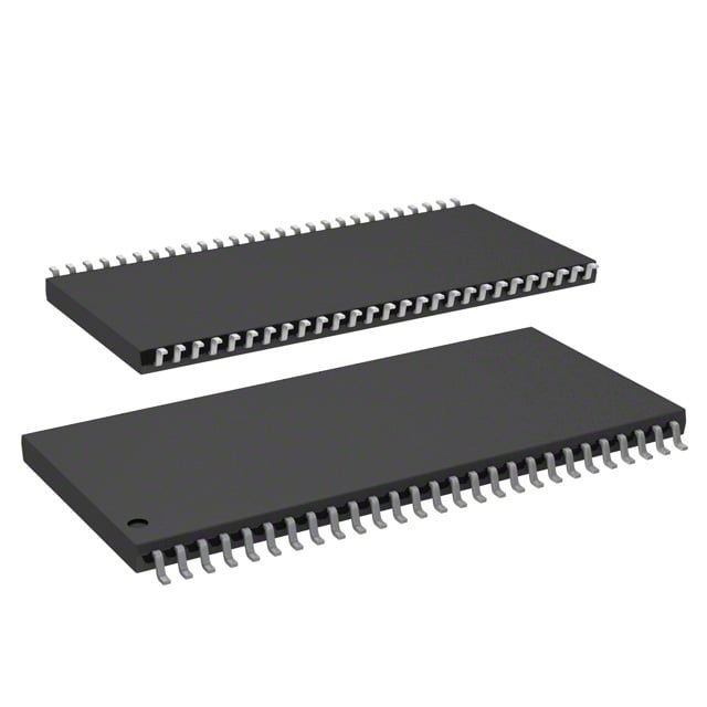
IC DRAM 64MBIT PAR 54TSOP II |
|---|---|
| Quantity | 897 Available (as of June 14, 2026) |
| Product Category | Memory |
|---|---|
| Manufacturer | Integrated Silicon Solution Inc |
| Manufacturing Status | Obsolete |
| Manufacturer Standard Lead Time | Contact Us |
| Datasheet |
Specifications & Environmental
| Device Package | 54-TSOP II | Memory Format | DRAM | Technology | SDRAM | ||
|---|---|---|---|---|---|---|---|
| Memory Size | 64 Mbit | Access Time | 5.4 ns | Grade | Industrial | ||
| Clock Frequency | 166 MHz | Voltage | 3V ~ 3.6V | Memory Type | Volatile | ||
| Operating Temperature | -40°C ~ 85°C (TA) | Write Cycle Time Word Page | N/A | Packaging | 54-TSOP (0.400", 10.16mm Width) | ||
| Mounting Method | Volatile | Memory Interface | Parallel | Memory Organization | 4M x 16 | ||
| Moisture Sensitivity Level | 3 (168 Hours) | RoHS Compliance | ROHS Compliant | REACH Compliance | REACH Unaffected | ||
| Qualification | N/A | ECCN | EAR99 | HTS Code | 8542.32.0002 |
Overview of IS45S16400F-6TLA1-TR – IC DRAM 64MBIT PAR 54TSOP II
The IS45S16400F-6TLA1-TR is a 64‑Mbit synchronous DRAM organized as 4M × 16 with 4 internal banks. It is a high‑speed, fully synchronous parallel DRAM designed for systems that require pipeline data transfer and configurable burst access.
This device targets designs that need a compact 54‑pin TSOP II footprint, 3.0–3.6 V supply compatibility, and industrial temperature operation, delivering flexible timing and refresh options for embedded and board‑level memory applications.
Key Features
- Core architecture – 1,048,576 × 16 × 4 banks (64 Mbit) organization with internal bank architecture for hiding row access and precharge.
- SDRAM technology – Fully synchronous DRAM with all signals referenced to the rising clock edge and LVTTL interface.
- Performance & timing – Rated clock frequency 166 MHz for this device variant; access time from clock (CAS latency = 3) is 5.4 ns.
- Burst and sequencing – Programmable burst length (1, 2, 4, 8, full page) and selectable burst sequence (sequential or interleave); supports burst read/write and burst read/single write operations.
- Refresh and self‑refresh – Auto refresh (CBR) and self‑refresh modes supported; 4096 refresh cycles every 64 ms for commercial/industrial grades as specified.
- Voltage and interface – Single 3.3 V nominal supply range (3.0 V to 3.6 V) with parallel memory interface.
- Package – 54‑pin TSOP II (0.400", 10.16 mm width) in a compact surface‑mount footprint.
- Operating temperature – Industrial range: −40 °C to +85 °C (TA).
Typical Applications
- Embedded systems – Provides external parallel SDRAM memory for microprocessor‑based boards requiring 64 Mbit storage in a small TSOP II package.
- Industrial controllers – Industrial temperature rating and self‑refresh support suit board‑level memory needs in factory and automation equipment.
- Buffering and frame storage – Programmable burst lengths and internal bank architecture enable burst buffering and block transfer operations in data buffering roles.
Unique Advantages
- Flexible burst control: Programmable burst length and sequence allow designers to optimize throughput for sequential or interleaved access patterns.
- Low latency option: CAS latency programmable (2 or 3 clocks) with measured access time of 5.4 ns at CAS = 3 for the −6 device variant.
- Compact, board‑friendly package: 54‑pin TSOP II (10.16 mm width) provides a small footprint for space‑constrained PCBs.
- Industrial temperature support: Rated for −40 °C to +85 °C to meet a wide range of ambient operating conditions.
- Standard 3.3 V operation: 3.0–3.6 V supply range simplifies integration into legacy 3.3 V power rails.
- Built‑in refresh handling: Auto refresh and self‑refresh modes reduce external refresh management and support low‑power idle states.
Why Choose IS45S16400F-6TLA1-TR?
The IS45S16400F-6TLA1-TR combines a 64‑Mbit SDRAM architecture with programmable latency, flexible burst control, and internal bank management to deliver predictable, synchronous memory performance in a compact TSOP II package. Its 3.3 V supply compatibility and industrial temperature range make it suitable for embedded and board‑level memory expansion where space and timing flexibility matter.
This device is well suited for designers seeking a parallel SDRAM solution with configurable performance parameters, robust refresh options, and a surface‑mount package for constrained PCBs, providing a clear and verifiable specification set for system integration.
If you need pricing or availability, request a quote or submit an RFQ to obtain current lead times and volume pricing information.