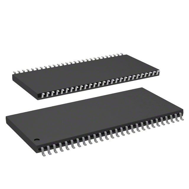
IS45S16400F-6TLA1
| Part Description |
IC DRAM 64MBIT PAR 54TSOP II |
|---|---|
| Quantity | 902 Available (as of June 15, 2026) |

| Product Category | Memory |
|---|---|
| Manufacturer | Integrated Silicon Solution Inc |
| Manufacturing Status | Obsolete |
| Manufacturer Standard Lead Time | Contact Us |
| Datasheet |
Specifications & Environmental
| Device Package | 54-TSOP II | Memory Format | DRAM | Technology | SDRAM | ||
|---|---|---|---|---|---|---|---|
| Memory Size | 64 Mbit | Access Time | 5.4 ns | Grade | Industrial | ||
| Clock Frequency | 166 MHz | Voltage | 3V ~ 3.6V | Memory Type | Volatile | ||
| Operating Temperature | -40°C ~ 85°C (TA) | Write Cycle Time Word Page | N/A | Packaging | 54-TSOP (0.400", 10.16mm Width) | ||
| Mounting Method | Volatile | Memory Interface | Parallel | Memory Organization | 4M x 16 | ||
| Moisture Sensitivity Level | 3 (168 Hours) | RoHS Compliance | ROHS Compliant | REACH Compliance | REACH Unaffected | ||
| Qualification | N/A | ECCN | EAR99 | HTS Code | 8542.32.0002 |
Overview of IS45S16400F-6TLA1 – IC DRAM 64MBIT PAR 54TSOP II
The IS45S16400F-6TLA1 is a 64‑Mbit synchronous DRAM organized as 1,048,576 × 16 × 4 banks. It implements a fully synchronous, pipelined architecture with internal banking to improve data throughput for parallel memory systems.
Targeted at designs that require high‑speed parallel SDRAM with a single 3.3 V supply and industrial temperature range, this device delivers programmable burst control, selectable CAS latency, and built‑in refresh/self‑refresh capabilities for robust system memory management.
Key Features
- Core & Memory Architecture Organized as 1,048,576 bits × 16 × 4 banks (4M × 16); internal bank architecture hides row access/precharge to improve effective throughput.
- Performance −6 speed grade supports a clock frequency of 166 MHz with an access time from clock of 5.4 ns (CAS latency = 3); programmable CAS latency options of 2 or 3 clocks.
- Interface & Burst Control Parallel memory interface with LVTTL signaling; programmable burst length (1, 2, 4, 8, full page) and selectable sequential or interleaved burst sequence for flexible data transfer patterns.
- Power & Refresh Single 3.3 V supply (operating range 3.0 V to 3.6 V); supports self‑refresh and auto refresh modes with 4096 refresh cycles per 64 ms (Com./Ind./A1) or 16 ms (A2) options documented in the device specification.
- Timing & Transfer Fully synchronous operation with all signals referenced to the rising clock edge; supports random column address every clock cycle and burst termination via burst stop or precharge command.
- Package & Temperature Range 54‑pin TSOP II package (0.400", 10.16 mm width) and documented industrial operating temperature range of −40 °C to +85 °C.
Typical Applications
- Embedded systems — Acts as parallel SDRAM for systems requiring 64‑Mbit external memory with high‑speed synchronous access and programmable burst modes.
- Industrial control — Suitable for control and automation equipment that requires operation across −40 °C to +85 °C with self‑refresh and auto‑refresh capabilities for stable operation.
- High‑speed buffering — Provides banked SDRAM architecture and pipeline timing for designs needing predictable, high‑rate data transfer and burst operations.
Unique Advantages
- Banked architecture for improved throughput: Four internal banks reduce the impact of row access/precharge delays and help maintain sustained data transfer rates.
- Flexible burst and latency control: Programmable burst lengths and CAS latency (2 or 3 clocks) allow tuning of read/write timing to match system requirements.
- Single‑supply, LVTTL interface: Operates from a 3.0 V to 3.6 V supply with LVTTL signaling to simplify power and interface design in 3.3 V systems.
- Industrial temperature support: Documented operation from −40 °C to +85 °C for deployment in temperature‑sensitive environments.
- Compact TSOP II footprint: 54‑pin TSOP II package (10.16 mm width) enables space‑conscious board layouts while providing a parallel SDRAM interface.
- Built‑in refresh management: Self‑refresh and auto‑refresh modes with defined refresh cycles support stable long‑term data retention without external intervention.
Why Choose IS45S16400F-6TLA1?
The IS45S16400F-6TLA1 combines a banked, pipelined SDRAM architecture with programmable timing and burst options to deliver a configurable 64‑Mbit parallel memory block suitable for systems that need predictable, synchronous data transfers. Its single 3.3 V supply, LVTTL interface, and industrial temperature rating make it appropriate for embedded and industrial designs that require reliable external DRAM.
Choose this device when your design requires a compact TSOP II package, selectable CAS latency, robust refresh capabilities, and a documented 166 MHz operating point (−6 speed grade) with a 5.4 ns access time from clock. Refer to the ISSI device specification for full electrical and timing details when integrating this memory into your system.
If you would like pricing, availability, or to request a quote for the IS45S16400F-6TLA1, please submit a request and our team will respond with the next steps and procurement options.