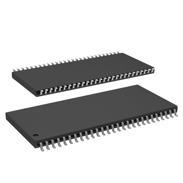
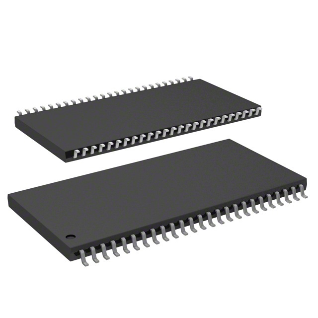
IS45S16400F-7TLA1
| Part Description |
IC DRAM 64MBIT PAR 54TSOP II |
|---|---|
| Quantity | 511 Available (as of June 15, 2026) |

| Product Category | DRAM Memory |
|---|---|
| Manufacturer | Integrated Silicon Solution Inc |
| Manufacturing Status | Obsolete |
| Manufacturer Standard Lead Time | Contact Us |
| Datasheet |
Specifications & Environmental
| Device Package | 54-TSOP II | Memory Format | DRAM | Technology | SDRAM | ||
|---|---|---|---|---|---|---|---|
| Memory Size | 64 Mbit | Access Time | 5.4 ns | Grade | Industrial | ||
| Clock Frequency | 143 MHz | Voltage | 3V ~ 3.6V | Memory Type | Volatile | ||
| Operating Temperature | -40°C ~ 85°C (TA) | Write Cycle Time Word Page | N/A | Packaging | 54-TSOP (0.400", 10.16mm Width) | ||
| Mounting Method | Volatile | Memory Interface | Parallel | Memory Organization | 4M x 16 | ||
| Moisture Sensitivity Level | 3 (168 Hours) | RoHS Compliance | ROHS Compliant | REACH Compliance | REACH Unaffected | ||
| Qualification | N/A | ECCN | EAR99 | HTS Code | 8542.32.0002 |
Overview of IS45S16400F-7TLA1 – IC DRAM 64MBIT PAR 54TSOP II
The IS45S16400F-7TLA1 is a 64‑Mbit synchronous dynamic RAM (SDRAM) organized as 1,048,576 × 16 × 4 banks with a parallel LVTTL interface. It implements a fully synchronous, pipelined architecture with internal banking to support high‑speed burst transfers.
This device is intended for designs that require a 64‑Mbit parallel SDRAM solution with programmable burst and CAS options, offering defined timing and refresh behavior for system memory and buffering applications.
Key Features
- Core Architecture Organized as 1,048,576 × 16 × 4 banks (4M × 16) to enable internal bank management for improved throughput and overlapped row operations.
- Memory Capacity & Format 64 Mbit DRAM capacity in a parallel memory format with 16‑bit data width.
- Performance Speed grade -7: clock frequency up to 143 MHz and CAS latency options (2 or 3); documented access time from clock of 5.4 ns for the -7 grade.
- Programmable Burst & Timing Programmable burst lengths (1, 2, 4, 8, full page) and burst sequence (sequential/interleave); burst termination via burst stop or precharge command; programmable CAS latency (2, 3 clocks).
- Refresh & Power Management Supports self‑refresh and auto refresh (CBR). Standard refresh count is 4,096 cycles per 64 ms (Com./Ind./A1 grades) or 4,096 per 16 ms for A2 grade.
- Voltage Supply Single 3.3 V supply behavior with an operating supply range documented as 3.0 V to 3.6 V.
- Interface Parallel LVTTL interface with all signals referenced to the positive clock edge for fully synchronous operation.
- Package & Temperature 54‑pin TSOP II package (0.400", 10.16 mm width) with specified operating ambient temperature range of -40°C to +85°C (TA).
Typical Applications
- Parallel SDRAM memory modules Use as a 64‑Mbit parallel SDRAM element where 16‑bit data paths and banked memory improve throughput.
- High‑speed data buffering Programmable burst lengths and internal bank architecture support burst read/write buffering and pipeline transfers.
- Embedded system memory expansion Compact TSOP II packaging and defined timing characteristics make the device suitable for space‑constrained board‑level memory designs.
Unique Advantages
- Configurable performance: Programmable CAS latency and burst length options allow tuning of read/write timing to match system requirements.
- Banked architecture for throughput: Four internal banks enable overlapping row accesses to minimize latency for burst transfers.
- Defined timing for system design: Documented clock frequency and access time for the -7 grade (143 MHz, 5.4 ns access from clock) simplify timing closure.
- Robust refresh support: Self‑refresh and auto refresh modes with specified refresh cycles provide predictable data retention behavior.
- Compact, industry‑standard package: 54‑pin TSOP II (10.16 mm width) supports board‑level integration where profile and footprint matter.
- Wide operating range: Supports a 3.0 V to 3.6 V supply range and industrial temperature operation down to -40°C.
Why Choose IS45S16400F-7TLA1?
The IS45S16400F-7TLA1 positions itself as a focused 64‑Mbit parallel SDRAM offering predictable, synchronous timing and flexible burst/CAS configurations. Its 4‑bank architecture, refresh modes, and LVTTL interface provide an implementation-ready memory block for designs that require defined performance and board‑level integration in a TSOP II package.
This device is suited to engineers specifying fixed‑capacity SDRAM with clear electrical and timing parameters, offering a balance of compact packaging, multiple timing options, and documented refresh behavior for reliable system memory and buffering functions.
Request a quote or submit an RFQ to receive pricing and availability information for IS45S16400F-7TLA1.