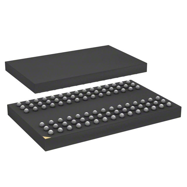
IS45S32400F-7BA25
| Part Description |
IC DRAM 128MBIT PAR 90TFBGA |
|---|---|
| Quantity | 1,714 Available (as of June 17, 2026) |

| Product Category | DRAM Memory |
|---|---|
| Manufacturer | Integrated Silicon Solution Inc |
| Manufacturing Status | Obsolete |
| Manufacturer Standard Lead Time | Contact Us |
| Datasheet |
Specifications & Environmental
| Device Package | 90-TFBGA (8x13) | Memory Format | DRAM | Technology | SDRAM | ||
|---|---|---|---|---|---|---|---|
| Memory Size | 128 Mbit | Access Time | 5.4 ns | Grade | Automotive | ||
| Clock Frequency | 143 MHz | Voltage | 3V ~ 3.6V | Memory Type | Volatile | ||
| Operating Temperature | -40°C ~ 105°C (TA) | Write Cycle Time Word Page | N/A | Packaging | 90-TFBGA | ||
| Mounting Method | Volatile | Memory Interface | Parallel | Memory Organization | 4M x 32 | ||
| Moisture Sensitivity Level | 3 (168 Hours) | RoHS Compliance | ROHS Compliant | REACH Compliance | REACH Unaffected | ||
| Qualification | N/A | ECCN | OBSOLETE | HTS Code | N/A |
Overview of IS45S32400F-7BA25 – IC DRAM 128MBIT PAR 90TFBGA
The IS45S32400F-7BA25 is a 128Mbit synchronous DRAM (SDRAM) organized as 4M × 32 with a quad-bank architecture and pipeline design for high-speed data transfer. It operates from a single 3.3V ±0.3V supply and provides a parallel LVTTL interface suitable for synchronous 3.3V memory subsystems.
Designed for applications requiring predictable synchronous access and flexible burst control, this device delivers programmable CAS latency, burst length and sequence, plus auto- and self-refresh options for reliable memory operation across a wide temperature range.
Key Features
- Core / Memory Organization – 128 Mbit SDRAM arranged as 4M × 32 with internal quad-bank structure to support pipelined, high-speed access.
- Performance – Clock frequency options include 166, 143 and 133 MHz; the -7 speed grade provides 143 MHz operation with a 5.4 ns access time (CAS latency = 3).
- Timing Flexibility – Programmable CAS latency (2 or 3 clocks), programmable burst length (1, 2, 4, 8, full page) and selectable sequential/interleave burst sequence.
- Refresh and Self-Refresh – Auto Refresh (CBR) and Self Refresh supported; refresh count options: 4K cycles every 16 ms (A2) or 64 ms (Commercial, Industrial, A1).
- Interface – Fully synchronous operation with all signals referenced to the rising clock edge and LVTTL compatible signaling; supports random column address every clock cycle.
- Power – Single power supply: 3.3V ±0.3V (specified voltage range 3.0V to 3.6V).
- Package & Mechanical – Available in a 90-ball TF-BGA package (90-TFBGA, 8 × 13) for compact board-level integration.
- Temperature Range – Specified operating temperature range includes down to −40°C; the part data lists operation up to 105°C (TA).
Typical Applications
- Synchronous 3.3V memory subsystems – Use as system DRAM where a 3.3V LVTTL synchronous interface and predictable timing are required.
- High‑speed buffer memory – Suitable for designs that need pipelined, burst-capable storage with programmable CAS latency and burst control.
- Temperature‑sensitive embedded systems – Applicable in designs that require validated operation across extended ambient temperatures.
Unique Advantages
- Quad‑bank pipelined architecture: Enables continuous high-speed transfers by hiding row access/precharge through internal banking.
- Flexible burst and timing control: Programmable burst length, sequence and CAS latency let designers tune throughput and latency to match system timing.
- Single‑supply simplicity: 3.3V ±0.3V single power rail reduces supply complexity for 3.3V memory systems.
- Compact TF‑BGA package: 90-ball TFBGA (8×13) provides a small footprint for space-constrained board designs.
- Robust refresh options: Auto and self‑refresh with selectable refresh intervals (4K cycles/16 ms or 64 ms) support different system refresh strategies.
Why Choose IC DRAM 128MBIT PAR 90TFBGA?
The IS45S32400F-7BA25 positions itself as a practical choice for designers who need a synchronous 128Mbit DRAM with flexible timing, burst control and a compact TF‑BGA footprint. Its quad-bank, pipelined architecture and LVTTL synchronous interface enable reliable, high-speed data transfers in 3.3V memory subsystems.
This device is suited to system-level memory designs that require programmable CAS latency and burst options, robust refresh modes and extended temperature operation. Technical documentation and device specifications provide the detail needed to integrate the IS45S32400F-7BA25 into board-level memory architectures.
Request a quote or submit a parts inquiry to evaluate IS45S32400F-7BA25 for your next design.