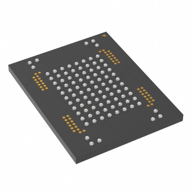
MT29F256G08AUCABH3-10ITZ:A
| Part Description |
IC FLASH 256GBIT PAR 100LBGA |
|---|---|
| Quantity | 1,299 Available (as of June 15, 2026) |
| Product Category | Memory |
|---|---|
| Manufacturer | Micron Technology Inc. |
| Manufacturing Status | Active |
| Manufacturer Standard Lead Time | 13 Weeks |
| Datasheet |
Specifications & Environmental
| Device Package | 100-LBGA (12x18) | Memory Format | FLASH | Technology | FLASH - NAND (SLC) | ||
|---|---|---|---|---|---|---|---|
| Memory Size | 256 Gbit | Access Time | N/A | Grade | Industrial | ||
| Clock Frequency | 100 MHz | Voltage | 2.7V ~ 3.6V | Memory Type | Non-Volatile | ||
| Operating Temperature | -40°C ~ 85°C (TA) | Write Cycle Time Word Page | N/A | Packaging | 100-LBGA | ||
| Mounting Method | Non-Volatile | Memory Interface | Parallel | Memory Organization | 32G x 8 | ||
| Moisture Sensitivity Level | 3 (168 Hours) | RoHS Compliance | ROHS3 Compliant | REACH Compliance | REACH Unaffected | ||
| Qualification | N/A | ECCN | 3A991B1A | HTS Code | 8542.32.0071 |
Overview of MT29F256G08AUCABH3-10ITZ:A – Parallel SLC NAND Flash 256Gbit, 100‑LBGA
The MT29F256G08AUCABH3-10ITZ:A is a 256 Gbit non-volatile Single-Level Cell (SLC) NAND flash device organized as 32G × 8 with a parallel interface. It implements ONFI 2.2-compliant command and I/O features and provides synchronous and asynchronous operation modes for embedded storage applications.
Targeted at designs that require high endurance, predictable program/erase characteristics and industrial temperature operation, this device delivers large capacity in a compact 100‑ball BGA (12×18) package while supporting advanced NAND commands and caching to improve throughput.
Key Features
- Memory Type & Organization Single-level cell (SLC) NAND flash, 256 Gbit total capacity organized as 32G × 8 with page size x8 = 8,640 bytes (8,192 + 448) and block size = 128 pages.
- Interface & Timing Parallel NAND interface with asynchronous and synchronous I/O; synchronous timing up to mode 5 and clock frequency listed at 100 MHz (DDR 10 ns timing).
- Performance Synchronous throughput up to 200 MT/s per pin and asynchronous throughput up to 50 MT/s per pin; typical array timings include read page 35 μs (max), program page 350 μs (typ), and erase block 1.5 ms (typ).
- Advanced Command Set ONFI 2.2-compliant command set with program cache, read cache (sequential and random), OTP mode, multi-plane and multi-LUN operations, copyback, and read unique ID.
- Power Operating VCC range 2.7–3.6 V; VCCQ supported at 1.7–1.95 V or 2.7–3.6 V as specified.
- Endurance & Reliability Endurance rated at 60,000 program/erase cycles and data retention compliant with JESD47G; operation status byte and hardware DQS strobes supported for data integrity and synchronization.
- Package & Temperature Available in a 100-ball BGA (100‑LBGA, 12×18) package and specified for industrial operating temperature range –40°C to +85°C (TA).
Typical Applications
- Industrial Embedded Systems SLC endurance and industrial temperature rating make the device suitable for embedded systems requiring long-life non-volatile storage.
- Data Logging and Energy Metering High program/erase endurance and robust data retention support repeated writes and long-term stored data in logging applications.
- Boot and System Storage Parallel NAND interface and ONFI command support enable use as primary or boot storage in appliances and network devices that utilize parallel flash.
Unique Advantages
- High Endurance SLC NAND: 60,000 program/erase cycles provide predictable longevity for write-intensive deployments.
- Dual I/O Modes: Both asynchronous and synchronous modes (ONFI 2.2) allow designers to balance compatibility and peak throughput up to 200 MT/s per pin in synchronous operation.
- Advanced Flash Controls: On-device program/read caches, multi-plane and multi-LUN commands, OTP and copyback operations increase effective throughput and flexibility for system-level flash management.
- Industrial Temperature Support: Specified –40°C to +85°C enables reliable operation across a wide temperature range for industrial-grade applications.
- Compact, High-Density Packaging: 256 Gbit capacity in a 100‑LBGA (12×18) package suits space-constrained board designs.
- Standards-Based Interface: ONFI 2.2 compliance and DQS strobe support provide standard, hardware-friendly synchronization for synchronous data transfers.
Why Choose IC FLASH 256GBIT PAR 100LBGA?
The MT29F256G08AUCABH3-10ITZ:A positions itself as a high-capacity, industrial-temperature SLC NAND solution with ONFI-compliant interfaces and advanced flash features that support predictable endurance and flexible performance modes. Its combination of 256 Gbit density, SLC endurance, and synchronous/asynchronous operation makes it suitable for embedded and industrial designs that require robust non‑volatile storage.
Designers seeking a compact, standards-based parallel NAND device will find the 100‑LBGA package, comprehensive command set, and documented timing and reliability characteristics helpful for system integration and long-term deployment.
Request a quote or submit an inquiry to receive pricing, availability, and additional technical information for MT29F256G08AUCABH3-10ITZ:A.