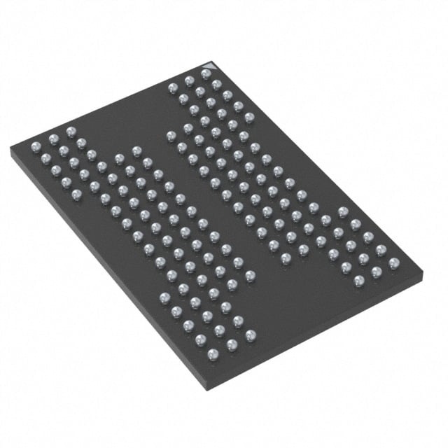
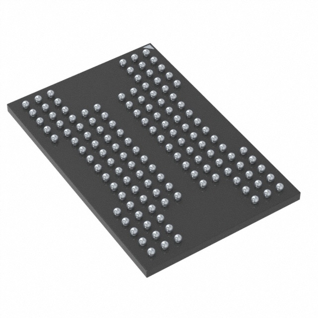
MT29F256G08AUCABJ3-10Z:A
| Part Description |
IC FLASH 256GBIT PAR 132LBGA |
|---|---|
| Quantity | 708 Available (as of June 18, 2026) |
| Product Category | Flash Memory |
|---|---|
| Manufacturer | Micron Technology Inc. |
| Manufacturing Status | Obsolete |
| Manufacturer Standard Lead Time | Contact Us |
| Datasheet |
Specifications & Environmental
| Device Package | 132-LBGA (12x18) | Memory Format | FLASH | Technology | FLASH - NAND (SLC) | ||
|---|---|---|---|---|---|---|---|
| Memory Size | 256 Gbit | Access Time | N/A | Grade | Commercial | ||
| Clock Frequency | 100 MHz | Voltage | 2.7V ~ 3.6V | Memory Type | Non-Volatile | ||
| Operating Temperature | 0°C ~ 70°C (TA) | Write Cycle Time Word Page | N/A | Packaging | N/A | ||
| Mounting Method | Non-Volatile | Memory Interface | Parallel | Memory Organization | 32G x 8 | ||
| Moisture Sensitivity Level | 3 (168 Hours) | RoHS Compliance | ROHS3 Compliant | REACH Compliance | REACH Unaffected | ||
| Qualification | N/A | ECCN | 3A991B1A | HTS Code | 8542.32.0071 |
Overview of MT29F256G08AUCABJ3-10Z:A – IC FLASH 256GBIT PAR 132LBGA
The MT29F256G08AUCABJ3-10Z:A is a 256 Gbit parallel NAND flash device from Micron Technology Inc., implemented with single-level cell (SLC) technology. It provides high-capacity, non-volatile storage in a 132-ball BGA (12×18) package for commercial-temperature embedded systems.
This device supports both synchronous and asynchronous I/O with ONFI 2.2 compliance and a range of advanced NAND commands, making it suitable for applications that require durable, high-throughput local storage and firmware/boot media in commercial equipment.
Key Features
- Memory Type & Capacity Non-volatile SLC NAND flash with a memory size of 256 Gbit organized as 32G × 8.
- Organization & Geometry Page size x8: 8,640 bytes (8,192 + 448); block size: 128 pages (1,024K + 56K bytes); plane size: 2 planes × 2,048 blocks per plane; 256Gb device = 32,768 blocks.
- Interface & Protocol Parallel memory interface with ONFI 2.2 compliance. Supports synchronous and asynchronous signaling and hardware data strobe (DQS) for synchronized data transfer.
- Performance Synchronous I/O up to timing mode 5 with DDR clock rate of 10 ns (read/write throughput per pin up to 200 MT/s). Asynchronous I/O up to timing mode 5 (read/write throughput per pin up to 50 MT/s). Typical array timings: read page 35 µs, program page 350 µs, erase block 1.5 ms.
- Voltage VCC operating range: 2.7 V to 3.6 V. VCCQ options: 1.7–1.95 V or 2.7–3.6 V.
- Reliability & Endurance Endurance rated at 60,000 program/erase cycles. Data retention is JESD47G compliant. Operation status byte provides software indications for operation completion, pass/fail, and write-protect status.
- Advanced Command Set Support for program cache, read cache (sequential and random), multi-plane and multi-LUN commands, OTP mode, read unique ID, and copyback. RESET (FFh) is required as first command after power-on.
- Package & Temperature Supplier device package: 132-LBGA (12×18). Specified operating temperature (TA): 0°C to +70°C.
Typical Applications
- Commercial Embedded Systems High-capacity non-volatile storage for embedded applications operating in commercial temperature ranges.
- Firmware and Boot Storage Reliable SLC storage for firmware images, boot code, and system recovery partitions where endurance and data retention are required.
- Data Logging and Local Media Local high-capacity storage for data buffering or logging in commercial devices that require frequent program/erase cycles and predictable performance.
- Consumer and Networking Devices Onboard non-volatile memory for consumer electronics and networking equipment that leverage parallel NAND performance and capacity.
Unique Advantages
- High Capacity in a Compact BGA 256 Gbit in a 132-ball BGA (12×18) footprint enables dense storage with a small board area impact.
- SLC Endurance 60,000 program/erase cycles provide longevity for applications with frequent write/erase activity.
- Flexible Performance Modes Support for synchronous DDR transfers (up to 200 MT/s per pin) and asynchronous modes allows designers to balance throughput and timing complexity.
- ONFI 2.2 Compliance Standardized interface and DQS support simplify integration with controllers that support ONFI-compliant NAND devices.
- Comprehensive Command Feature Set Program/read caches, multi-plane and multi-LUN operations, OTP mode, and copyback operations enable optimized flash management and system-level performance strategies.
- Robust Data Retention JESD47G-compliant data retention helps meet reliability expectations for commercial applications.
Why Choose MT29F256G08AUCABJ3-10Z:A?
The MT29F256G08AUCABJ3-10Z:A positions itself as a high-capacity, high-endurance SLC NAND solution for commercial embedded designs that require reliable non-volatile storage with flexible performance modes. Its ONFI 2.2-compliant parallel interface, advanced command set, and documented array timings provide predictable integration and system-level behavior.
This Micron device is suited to designers who need scalable storage capacity, standardized interfaces, and endurance characteristics for firmware, boot, and local data storage in commercial-temperature equipment. The combination of SLC endurance, JESD47G data retention compliance, and a compact 132-LBGA package supports durable, long-life deployments where component-level reliability matters.
Request a quote or contact sales to discuss availability, lead times, and how this part fits your commercial embedded storage requirements.