MT29F256G08CJABAWP:B TR
| Part Description |
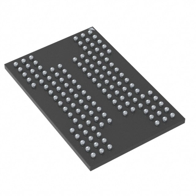
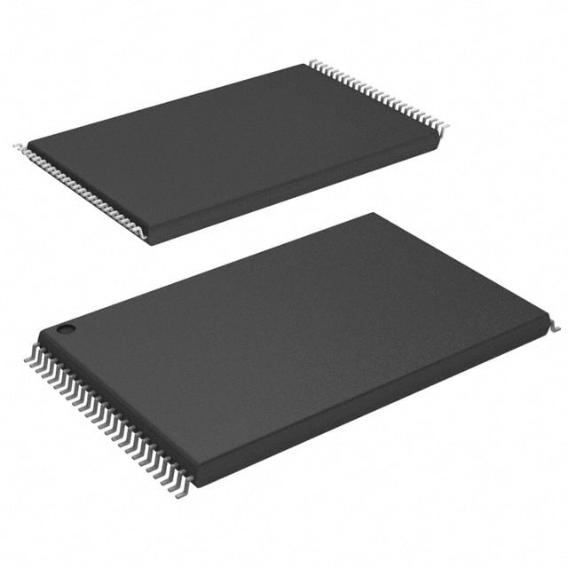
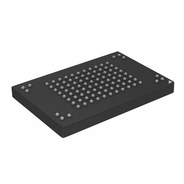
IC FLASH 256GBIT PAR 48TSOP I |
|---|---|
| Quantity | 734 Available (as of June 15, 2026) |

| Product Category | Flash Memory |
|---|---|
| Manufacturer | Micron Technology Inc. |
| Manufacturing Status | Obsolete |
| Manufacturer Standard Lead Time | Contact Us |
| Datasheet |
Specifications & Environmental
| Device Package | 48-TSOP I | Memory Format | FLASH | Technology | FLASH - NAND (MLC) | ||
|---|---|---|---|---|---|---|---|
| Memory Size | 256 Gbit | Access Time | N/A | Grade | Commercial | ||
| Clock Frequency | N/A | Voltage | 2.7V ~ 3.6V | Memory Type | Non-Volatile | ||
| Operating Temperature | 0°C ~ 70°C (TA) | Write Cycle Time Word Page | N/A | Packaging | 48-TFSOP (0.724", 18.40mm Width) | ||
| Mounting Method | Non-Volatile | Memory Interface | Parallel | Memory Organization | 32G x 8 | ||
| Moisture Sensitivity Level | 3 (168 Hours) | RoHS Compliance | ROHS3 Compliant | REACH Compliance | REACH Unaffected | ||
| Qualification | N/A | ECCN | 3A991B1A | HTS Code | 8542.32.0071 |
Overview of MT29F256G08CJABAWP:B TR – IC FLASH 256GBIT PAR 48TSOP I
The MT29F256G08CJABAWP:B TR is a 256 Gbit non-volatile NAND flash memory device from Micron Technology Inc., implemented as MLC (Multi-Level Cell) NAND. It provides a parallel memory interface and a 32G × 8 memory organization in a 48-TSOP I package, designed for system designs that require high-density parallel flash storage.
Key attributes include a 256 Gbit capacity, parallel interface, support for 2.7 V to 3.6 V supply rails, and an operating ambient temperature range of 0°C to 70°C—suitable where this combination of density, package, and voltage compatibility is required.
Key Features
- Memory Technology NAND flash (MLC) non-volatile memory offering a 256 Gbit storage capacity in a 32G × 8 organization.
- Interface Parallel memory interface for integration with parallel memory controllers and legacy parallel bus designs.
- Voltage Operates from 2.7 V to 3.6 V, supporting common 3.3 V system power rails.
- Package 48-TSOP I / 48-TFSOP (0.724", 18.40 mm width) surface-mount package for board-level density and standard TSOP footprint placement.
- Operating Temperature Specified for ambient operation from 0°C to 70°C (TA), suitable for standard commercial temperature environments.
- Memory Format & Organization FLASH memory formatted as 32G × 8, enabling byte-wide parallel access patterns.
Typical Applications
- Embedded storage systems High-density non-volatile storage for embedded controllers and subsystems that require large local data or firmware storage in a parallel flash form factor.
- Consumer electronics Provides large-capacity parallel flash memory in devices where a 48-TSOP footprint and 3.3 V-compatible supply are required.
- Data logging and media storage Suitable for designs needing substantial on-board non-volatile capacity with parallel access for bulk data retention and retrieval.
Unique Advantages
- High density 256 Gbit capacity: Enables substantial on-board storage without multiple devices, reducing board area and BOM complexity.
- Parallel interface: Simplifies integration with parallel memory controllers and legacy parallel bus architectures.
- Standard 48-TSOP I package: Compact, industry-familiar footprint eases PCB layout and assembly using established TSOP processes.
- Wide supply compatibility: 2.7 V to 3.6 V range allows direct use with common 3.3 V systems and power domains.
- Commercial temperature rating: Specified 0°C to 70°C operation aligns with many consumer and commercial product requirements.
- MLC NAND technology: Multi-level cell implementation provides higher bit density per die for increased storage capacity.
Why Choose IC FLASH 256GBIT PAR 48TSOP I?
MT29F256G08CJABAWP:B TR positions itself as a high-density, parallel NAND flash option in a standard 48-TSOP I package from Micron Technology Inc. It is suitable for engineers and procurement teams seeking a 256 Gbit non-volatile memory device that matches 3.3 V system architectures and requires commercial temperature operation.
Designs that need large byte-wide flash capacity, straightforward board-level integration, and a familiar TSOP footprint can leverage this device to consolidate storage and simplify layout. The combination of MLC NAND technology, defined memory organization, and standard package dimensions supports scalable implementations where capacity and package compatibility are primary selection criteria.
Request a quote or submit an inquiry for MT29F256G08CJABAWP:B TR to check availability, lead times, and pricing for your design requirements.