MT29F256G08CJABBWP-12:B
| Part Description |
IC FLASH 256GBIT PAR 48TSOP I |
|---|---|
| Quantity | 975 Available (as of June 15, 2026) |

| Product Category | Flash Memory |
|---|---|
| Manufacturer | Micron Technology Inc. |
| Manufacturing Status | Obsolete |
| Manufacturer Standard Lead Time | Contact Us |
| Datasheet |
Specifications & Environmental
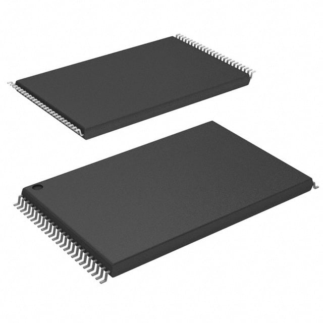
| Device Package | 48-TSOP I | Memory Format | FLASH | Technology | FLASH - NAND (MLC) | ||
|---|---|---|---|---|---|---|---|
| Memory Size | 256 Gbit | Access Time | N/A | Grade | Commercial | ||
| Clock Frequency | 83 MHz | Voltage | 2.7V ~ 3.6V | Memory Type | Non-Volatile | ||
| Operating Temperature | 0°C ~ 70°C (TA) | Write Cycle Time Word Page | N/A | Packaging | 48-TFSOP (0.724", 18.40mm Width) | ||
| Mounting Method | Non-Volatile | Memory Interface | Parallel | Memory Organization | 32G x 8 | ||
| Moisture Sensitivity Level | 3 (168 Hours) | RoHS Compliance | ROHS3 Compliant | REACH Compliance | REACH Unaffected | ||
| Qualification | N/A | ECCN | 3A991B1A | HTS Code | 8542.32.0071 |
Overview of MT29F256G08CJABBWP-12:B – IC FLASH 256GBIT PAR 48TSOP I
The MT29F256G08CJABBWP-12:B is a 256 Gbit non-volatile NAND flash memory organized as 32G × 8 and implemented in MLC (multi-level cell) technology. It provides a parallel memory interface and is offered in a 48‑TSOP I package for board-level integration.
Designed for systems that require high-density parallel flash storage within a compact package, this device operates from a 2.7 V to 3.6 V supply and supports operation across a 0 °C to 70 °C ambient temperature range.
Key Features
- Memory Type & Technology Non-volatile NAND flash using MLC technology for multi-bit storage per cell.
- Density & Organization 256 Gbit capacity with a 32G × 8 memory organization.
- Interface Parallel memory interface for direct parallel connection to compatible system controllers.
- Clock Frequency Supports a clock frequency of 83 MHz for synchronous operation with compatible host timing.
- Voltage Supply Operates from 2.7 V to 3.6 V, enabling use in 3.0 V-class systems.
- Package 48‑TSOP I (48‑TFSOP, 0.724" / 18.40 mm width) package suitable for surface-mount PCB assembly.
- Operating Temperature Specified for ambient operation from 0 °C to 70 °C (TA).
Unique Advantages
- High storage density: 256 Gbit capacity supports large data storage requirements within a single device, reducing board-level part count.
- Parallel interface simplicity: The parallel memory interface provides a straightforward integration path with parallel host controllers and legacy systems.
- Wide supply range: 2.7 V to 3.6 V support accommodates common 3.0 V system rails for flexible power design.
- Compact TSOP package: 48‑TSOP I package balances footprint and ease of assembly for space-constrained PCBs.
- Specified operating range: Operation guaranteed across 0 °C to 70 °C enables deployment in standard commercial temperature environments.
Why Choose MT29F256G08CJABBWP-12:B?
The MT29F256G08CJABBWP-12:B positions itself as a high-density, parallel NAND flash memory option for designs that require large non-volatile storage in a compact 48‑TSOP footprint. Its 32G × 8 organization, MLC technology, and 2.7 V–3.6 V supply support integration into a range of commercial electronic systems.
This device is suited for customers and designs that prioritize capacity, straightforward parallel interfacing, and standard commercial temperature operation, offering a component-level solution that simplifies BOM and layout considerations while meeting defined electrical and thermal specifications.
Request a quote or contact sales to discuss pricing, availability, and technical support for the MT29F256G08CJABBWP-12:B.