MT29F32G08ABAAAWP:A TR
| Part Description |
IC FLASH 32GBIT PAR 48TSOP I |
|---|---|
| Quantity | 148 Available (as of June 15, 2026) |

| Product Category | Flash Memory |
|---|---|
| Manufacturer | Micron Technology Inc. |
| Manufacturing Status | Obsolete |
| Manufacturer Standard Lead Time | Contact Us |
| Datasheet |
Specifications & Environmental
| Device Package | 48-TSOP I | Memory Format | FLASH | Technology | FLASH - NAND | ||
|---|---|---|---|---|---|---|---|
| Memory Size | 32 Gbit | Access Time | N/A | Grade | Commercial | ||
| Clock Frequency | N/A | Voltage | 2.7V ~ 3.6V | Memory Type | Non-Volatile | ||
| Operating Temperature | 0°C ~ 70°C (TA) | Write Cycle Time Word Page | N/A | Packaging | 48-TFSOP (0.724", 18.40mm Width) | ||
| Mounting Method | Non-Volatile | Memory Interface | Parallel | Memory Organization | 4G x 8 | ||
| Moisture Sensitivity Level | 3 (168 Hours) | RoHS Compliance | ROHS3 Compliant | REACH Compliance | REACH Unknown | ||
| Qualification | N/A | ECCN | 3A991B1A | HTS Code | 8542.32.0071 |
Overview of MT29F32G08ABAAAWP:A TR – IC FLASH 32GBIT PAR 48TSOP I
The MT29F32G08ABAAAWP:A TR is a 32 Gbit non-volatile NAND flash memory device in a 48-TSOP I package. It implements SLC NAND architecture with parallel and synchronous/asynchronous I/O options, designed for applications requiring high-endurance, on-board flash storage in a commercial temperature range.
Key Features
- Memory Type & Capacity — 32 Gbit NAND flash organized as 4G × 8, with page size 8,640 bytes (8,192 + 448 bytes) and block size of 128 pages.
- Technology — Single-level cell (SLC) NAND offering the endurance characteristics specified in the datasheet.
- Interface — Parallel memory interface supporting both asynchronous and synchronous modes and ONFI 2.2-compliant command set.
- Performance (Synchronous) — Synchronous I/O up to timing mode 5 with DDR clock rate 10 ns and read/write throughput per pin up to 200 MT/s; data strobe (DQS) signals provided for synchronous data alignment.
- Performance (Asynchronous) — Asynchronous I/O up to timing mode 5 with read/write throughput per pin up to 50 MT/s; typical array timings include read page 35 µs (max), program page 350 µs (typ), and erase block 1.5 ms (typ).
- Power — Operating supply voltage range VCC: 2.7–3.6 V; VCCQ supported at 1.7–1.95 V and 2.7–3.6 V.
- Advanced Command Set — Supports program cache, read cache (sequential and random), OTP mode, multi-plane and multi-LUN operations, read unique ID, and copyback operations.
- Reliability & Endurance — Endurance rated at 80,000 program/erase cycles; data retention compliant with JESD47G as noted in the datasheet.
- Operational Notes — RESET (FFh) is required as the first command after power-on; operation status byte provides software methods to detect operation completion and pass/fail conditions.
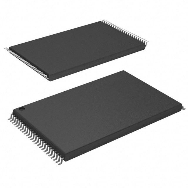
- Package & Temperature — Supplied in a 48-TSOP I (48-TFSOP, 0.724" / 18.40 mm width) package and specified for commercial operation from 0°C to +70°C.
Unique Advantages
- ONFI 2.2 Compliance: Ensures a standardized NAND command and timing interface for interoperability with compatible controllers.
- SLC Endurance: 80,000 program/erase cycles provide a measurable endurance profile suitable for write-intensive storage use cases.
- Flexible I/O Modes: Support for both asynchronous and high-speed synchronous DDR modes (with DQS) enables designers to balance throughput and system complexity.
- Comprehensive Command Set: Built-in features such as multi-plane commands, program/read caches, and OTP mode enable advanced flash management and efficient data handling.
- Wide Supply Options: Multiple VCCQ options (1.7–1.95 V and 2.7–3.6 V) and VCC 2.7–3.6 V allow compatibility with a range of system voltage domains.
Why Choose IC FLASH 32GBIT PAR 48TSOP I?
The MT29F32G08ABAAAWP:A TR delivers a 32 Gbit SLC NAND flash solution that combines high endurance, flexible I/O modes, and a compact 48-TSOP I package for commercial-temperature embedded storage designs. Its ONFI 2.2 compliance and advanced command features enable robust integration into systems that require deterministic flash behavior and software-managed status reporting.
This device is appropriate for designs that need proven endurance and predictable array performance (read, program, erase timing) while operating within a 0°C to +70°C ambient range. The combination of synchronous DDR capability and comprehensive flash commands supports scalable throughput and efficient memory management in board-level implementations.
Request a quote or submit an inquiry to obtain pricing, lead times, and availability for the MT29F32G08ABAAAWP:A TR.