MT29F32G08ABAAAWP:A
| Part Description |
IC FLASH 32GBIT PAR 48TSOP I |
|---|---|
| Quantity | 8 Available (as of June 9, 2026) |

| Product Category | Memory |
|---|---|
| Manufacturer | Micron Technology Inc. |
| Manufacturing Status | Obsolete |
| Manufacturer Standard Lead Time | Contact Us |
| Datasheet |
Specifications & Environmental
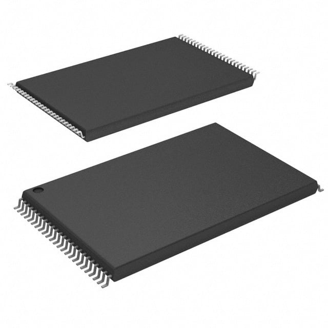
| Device Package | 48-TSOP I | Memory Format | FLASH | Technology | FLASH - NAND | ||
|---|---|---|---|---|---|---|---|
| Memory Size | 32 Gbit | Access Time | N/A | Grade | Commercial | ||
| Clock Frequency | N/A | Voltage | 2.7V ~ 3.6V | Memory Type | Non-Volatile | ||
| Operating Temperature | 0°C ~ 70°C (TA) | Write Cycle Time Word Page | N/A | Packaging | 48-TFSOP (0.724", 18.40mm Width) | ||
| Mounting Method | Non-Volatile | Memory Interface | Parallel | Memory Organization | 4G x 8 | ||
| Moisture Sensitivity Level | 3 (168 Hours) | RoHS Compliance | ROHS3 Compliant | REACH Compliance | REACH Unknown | ||
| Qualification | N/A | ECCN | 3A991B1A | HTS Code | 8542.32.0071 |
Overview of MT29F32G08ABAAAWP:A – IC FLASH 32GBIT PAR 48TSOP I
The MT29F32G08ABAAAWP:A is a 32 Gbit parallel NAND flash memory device in a 48‑pin TSOP I package. It implements asynchronous and synchronous NAND architectures with ONFI 2.2‑compliant signaling and supports a parallel x8 organization (4G × 8).
Designed for embedded non‑volatile storage, the device provides multi‑mode I/O, a comprehensive command set and defined array performance characteristics to support system designs requiring deterministic program/read/erase behavior and flexible interface options.
Key Features
- Memory Capacity & Organization 32 Gbit total density organized as 4G × 8 with 4096 total blocks (device size listing from the product family).
- Page, Block and Plane Geometry Page size (×8): 8640 bytes (8192 + 448); block size: 128 pages; plane configuration: 2 planes × 2048 blocks per plane.
- Synchronous and Asynchronous I/O Supports synchronous timing up to mode 5 with DQS data strobes and asynchronous timing up to mode 5. Read/write throughput per pin: up to 200 MT/s (synchronous) and 50 MT/s (asynchronous).
- Array Performance Specified timings include read page ≤ 35 μs (MAX), program page ~350 μs (TYP), and block erase ~1.5 ms (TYP).
- Command Set & Advanced Operations ONFI NAND Flash Protocol, plus advanced commands: program cache, read cache (sequential and random), OTP mode, multi‑plane commands, multi‑LUN operations, read unique ID and copyback.
- Endurance & Data Retention Endurance specified at 80,000 program/erase cycles and data retention compliant with JESD47G (per datasheet family notes).
- Power and Voltage Operating VCC range 2.7–3.6 V. VCCQ supported at 1.7–1.95 V or 2.7–3.6 V per device options.
- Package and Temperature 48‑TSOP I (48‑TFSOP, 18.40 mm width) package; commercial operating temperature 0°C to +70°C (TA).
- System Integration Notes RESET (FFh) is required as the first command after power‑on; the operation status byte provides software methods to detect completion, pass/fail and write‑protect status. First block (block address 00h) is valid when shipped from factory.
Typical Applications
- Embedded non‑volatile storage systems Use the MT29F32G08ABAAAWP:A where parallel NAND x8 storage with defined page/block geometry is required for firmware, code storage, or file systems.
- Systems requiring deterministic program/read/erase timing The specified array performance numbers (read, program, erase) support designs that need predictable flash operation latencies.
- Designs needing flexible I/O modes Applications that can benefit from either asynchronous or synchronous I/O operation and ONFI 2.2 interoperability.
Unique Advantages
- High density in a compact TSOP package: 32 Gbit capacity in a 48‑TSOP I footprint enables significant storage without large PCB area changes.
- Flexible interface modes: Support for both asynchronous and synchronous operation (with DQS) and ONFI 2.2 compliance allows integration into a range of parallel NAND host controllers.
- Advanced command capabilities: Program/read cache, multi‑plane and multi‑LUN commands and OTP mode provide functionality to optimize throughput and storage management.
- Defined endurance and retention: Endurance of 80,000 program/erase cycles and JESD47G data retention compliance provide quantified reliability characteristics for lifecycle planning.
- Predictable array performance: Published read, program and erase timings support system timing budgets and performance analysis.
- Power and voltage flexibility: VCC and VCCQ options cover common system supply ranges (2.7–3.6 V and 1.7–1.95 V) for varied host designs.
Why Choose MT29F32G08ABAAAWP:A?
The MT29F32G08ABAAAWP:A combines a high 32 Gbit density with ONFI 2.2‑compliant parallel interfaces and a compact 48‑TSOP package to deliver a practical, quantifiable NAND flash solution for embedded storage applications. Its documented array performance, advanced command set and endurance/retention specifications make it suitable for designs that require stable, predictable non‑volatile storage behavior.
This device is well suited to engineering teams and procurement seeking a parallel x8 NAND memory device with defined electrical, timing and reliability parameters, and where integration into existing NAND‑based architectures and host controllers is required.
Request a quote or submit an inquiry to obtain pricing, lead time and ordering information for MT29F32G08ABAAAWP:A.