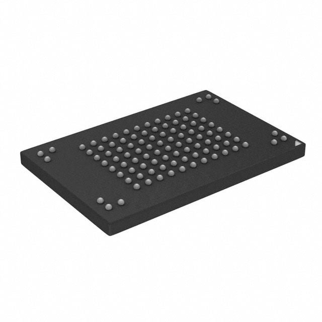
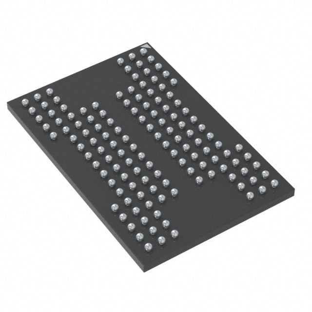
MT29F32G08AECBBH1-12:B TR
| Part Description |
IC FLASH 32GBIT PARALLEL 100VBGA |
|---|---|
| Quantity | 411 Available (as of June 17, 2026) |

| Product Category | Flash Memory |
|---|---|
| Manufacturer | Micron Technology Inc. |
| Manufacturing Status | Obsolete |
| Manufacturer Standard Lead Time | Contact Us |
| Datasheet |
Specifications & Environmental
| Device Package | 100-VBGA (12x18) | Memory Format | FLASH | Technology | FLASH - NAND | ||
|---|---|---|---|---|---|---|---|
| Memory Size | 32 Gbit | Access Time | N/A | Grade | Commercial | ||
| Clock Frequency | 83 MHz | Voltage | 2.7V ~ 3.6V | Memory Type | Non-Volatile | ||
| Operating Temperature | 0°C ~ 70°C (TA) | Write Cycle Time Word Page | N/A | Packaging | 100-VBGA | ||
| Mounting Method | Non-Volatile | Memory Interface | Parallel | Memory Organization | 4G x 8 | ||
| Moisture Sensitivity Level | 3 (168 Hours) | RoHS Compliance | ROHS3 Compliant | REACH Compliance | REACH Unknown | ||
| Qualification | N/A | ECCN | 3A991B1A | HTS Code | 8542.32.0071 |
Overview of MT29F32G08AECBBH1-12:B TR – IC FLASH 32GBIT PARALLEL 100VBGA
The MT29F32G08AECBBH1-12:B TR is a 32 Gbit non-volatile NAND flash memory device in a 100-ball VBGA (12×18) package. It implements NAND FLASH technology with a parallel interface and is intended for high-density embedded storage applications requiring SLC-based flash architecture.
Designed for applications that need compact, high-capacity NAND in a solder-down BGA footprint, the device provides a range of synchronous and asynchronous I/O modes along with Micron’s NAND command set and advanced data management features.
Key Features
- Memory Core — 32 Gbit NAND flash organized as 4G × 8, with 4096 blocks per device (32Gb density).
- Cell Technology — Single-level cell (SLC) NAND technology as specified in the device datasheet.
- Organization and Geometry — Page size (×8): 8640 bytes (8192 + 448); block size: 128 pages; plane structure: 2 planes × 2048 blocks per plane.
- Interface and Timing — Parallel NAND interface with support for asynchronous and synchronous I/O; ONFI 2.2-compliant operation per the datasheet. Clock frequency specified as 83 MHz in device data.
- Performance Characteristics — Synchronous throughput up to 200 MT/s per pin (DDR timing modes); asynchronous throughput up to 50 MT/s per pin; typical array timings include read page (35 µs), program page (350 µs), and erase block (1.5 ms) as listed in the datasheet.
- Voltage and Power — Operating supply range VCC: 2.7–3.6 V; VCCQ options noted in the datasheet (1.7–1.95 V or 2.7–3.6 V depending on configuration).
- Package — 100-ball VBGA package (12×18 mm ball grid array) for compact board-level integration.
- Operating Temperature — Commercial temperature range: 0°C to +70°C (TA).
- Advanced Command Set — Supports program cache, read cache (sequential and random), multi-plane commands, multi-LUN operations, copyback, OTP mode, read unique ID, and standard ONFI commands; RESET (FFh) required as first command after power-on.
- Reliability — Endurance rated at 80,000 program/erase cycles and data retention compliant with JESD47G per the datasheet.
Typical Applications
- Embedded Storage — High-density, soldered NAND for firmware, file systems, and local data storage in embedded platforms.
- Consumer and Connected Devices — On-board non-volatile storage for set-top boxes, media devices, and consumer electronics requiring compact 32 Gbit memory.
- Networking and Infrastructure — Boot and data storage in network appliances and communications equipment where compact BGA packaging and SLC endurance are required.
Unique Advantages
- High Density in a Small Footprint: 32 Gbit capacity in a 100-ball VBGA (12×18) package reduces board area compared to discrete solutions.
- Flexible Interface Modes: Support for both asynchronous and synchronous (ONFI 2.2) I/O enables designers to select the timing mode that matches system performance and design constraints.
- SLC Endurance: Single-level cell technology with an endurance specification of 80,000 program/erase cycles provides longevity for write-intensive applications.
- Advanced Command and Cache Support: Program cache, read cache, multi-plane and copyback operations improve effective throughput and internal data management.
- Wide Operating Voltage Range: 2.7–3.6 V supply range supports common system power rails for easy integration.
- Deterministic Array Timing: Published typical and maximum timings (read, program, erase) aid system-level timing and performance planning.
Why Choose IC FLASH 32GBIT PARALLEL 100VBGA?
The MT29F32G08AECBBH1-12:B TR is positioned as a compact, high-density NAND flash device that combines SLC reliability with a parallel interface and advanced NAND command features. Its package, voltage range, and documented array timings make it suitable for embedded and infrastructure designs that require on-board, soldered non-volatile storage.
Engineers specifying this device benefit from Micron’s documented endurance and data retention metrics, a comprehensive command set for performance tuning, and a package optimized for space-constrained board designs.
Request a quote or submit a pricing and availability inquiry to evaluate MT29F32G08AECBBH1-12:B TR for your next design.