MT29F32G08AECCBH1-10Z:C TR
| Part Description |
IC FLASH 32GBIT PARALLEL 100VBGA |
|---|---|
| Quantity | 214 Available (as of June 18, 2026) |

| Product Category | Flash Memory |
|---|---|
| Manufacturer | Micron Technology Inc. |
| Manufacturing Status | Obsolete |
| Manufacturer Standard Lead Time | Contact Us |
| Datasheet |
Specifications & Environmental
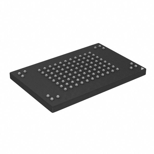
| Device Package | 100-VBGA (12x18) | Memory Format | FLASH | Technology | FLASH - NAND | ||
|---|---|---|---|---|---|---|---|
| Memory Size | 32 Gbit | Access Time | N/A | Grade | Commercial | ||
| Clock Frequency | 100 MHz | Voltage | 2.7V ~ 3.6V | Memory Type | Non-Volatile | ||
| Operating Temperature | 0°C ~ 70°C (TA) | Write Cycle Time Word Page | N/A | Packaging | 100-VBGA | ||
| Mounting Method | Non-Volatile | Memory Interface | Parallel | Memory Organization | 4G x 8 | ||
| Moisture Sensitivity Level | 3 (168 Hours) | RoHS Compliance | ROHS Compliant | REACH Compliance | REACH Unaffected | ||
| Qualification | N/A | ECCN | 3A991B1A | HTS Code | 8542.32.0071 |
Overview of MT29F32G08AECCBH1-10Z:C TR – IC FLASH 32GBIT PARALLEL 100VBGA
The MT29F32G08AECCBH1-10Z:C TR is a 32 Gbit non-volatile NAND flash memory device organized as 4G × 8 with a parallel memory interface. It is packaged in a 100-ball VBGA (12 × 18) and operates from a 2.7 V to 3.6 V supply with an ambient operating temperature range of 0 °C to 70 °C.
This device implements NAND flash architecture with advanced command capabilities and is designed for designs requiring on‑board parallel NAND storage in a compact BGA package, providing endurance and data-retention characteristics appropriate for long-term non-volatile storage.
Key Features
- Memory Type & Capacity — 32 Gbit NAND flash organized as 4G × 8 (FLASH memory format).
- Packaging — 100-ball VBGA package (12 × 18) for compact board-level integration.
- Interface & Clock — Parallel memory interface with a specified clock frequency of 100 MHz.
- Voltage Supply — Operates from VCC 2.7 V to 3.6 V. VCCQ options include 1.7–1.95 V or 2.7–3.6 V (per device datasheet).
- ONFI Compliance & Synchronous/Asynchronous Modes — ONFI 2.2-compliant device supporting both synchronous and asynchronous I/O; synchronous operation supports higher transfer rates and DQS data strobe for data synchronization.
- Performance (from datasheet) — Synchronous read/write throughput per pin up to 200 MT/s (DDR mode); asynchronous throughput per pin up to 50 MT/s; synchronous timing up to mode 5.
- Memory Geometry & Performance Details — Page size x8: 8640 bytes (8192 + 448); block size: 128 pages; plane and device block organization documented in the datasheet.
- Advanced Command Set — Program cache, read cache (sequential and random), OTP mode, multi‑plane commands, multi‑LUN operations, read unique ID, and copyback operations.
- Reliability & Endurance — Data retention compliant with JESD47G and endurance specified at 80,000 program/erase cycles (per datasheet).
- Power-On & Initialization — RESET (FFh) required as the first command after power-on; first block (block address 00h) is valid when shipped from the factory.
- Operating Conditions — Commercial temperature grade: 0 °C to +70 °C (TA).
Typical Applications
- Board‑level Parallel NAND Storage — Integration where a compact 100‑ball VBGA parallel NAND device is required for on‑board non‑volatile memory.
- Embedded Systems — Systems that need a 32 Gbit NAND device with advanced command features such as program/read caching and multi‑plane operations.
- Long‑term Non‑Volatile Storage — Designs demanding documented endurance and data retention characteristics (JESD47G compliance and 80,000 P/E cycles as specified).
Unique Advantages
- High Density in a Compact Package: 32 Gbit capacity in a 100‑VBGA (12×18) reduces PCB area for high-capacity on‑board storage.
- Flexible Interface Modes: ONFI 2.2 compliance with both synchronous and asynchronous modes enables designers to choose performance vs. system complexity trade-offs.
- Advanced Command Support: Program/read cache, multi‑plane and multi‑LUN commands, OTP and copyback simplify data management and can improve throughput in multi‑block operations.
- Documented Endurance and Retention: Specified 80,000 program/erase cycles and JESD47G data retention information support reliability planning for long‑lived storage designs.
- Standard Supply and Initialization Behavior: Defined VCC/VCCQ ranges and required RESET-on-power-on behavior provide clear integration and power sequencing requirements.
- Factory‑Valid First Block: First block (block address 00h) is valid at shipment, simplifying initial device use and validation.
Why Choose MT29F32G08AECCBH1-10Z:C TR?
The MT29F32G08AECCBH1-10Z:C TR delivers 32 Gbit of parallel NAND flash in a space‑efficient 100‑ball VBGA package with documented endurance and data retention characteristics. Its ONFI 2.2 compliance, synchronous/asynchronous interface flexibility, and advanced command set make it suitable for designs that require predictable NAND behavior, on‑board storage density, and features to optimize throughput and data management.
This device is appropriate for designers specifying commercial temperature operation (0 °C to 70 °C) and a 2.7–3.6 V power domain. The combination of compact packaging, interface options, and endurance data supports scalable, robust embedded storage implementations where verified NAND characteristics are required.
Request a quote or submit an inquiry for pricing, availability and lead time information for MT29F32G08AECCBH1-10Z:C TR.