MT29F32G08AFABAWP:B TR
| Part Description |
IC FLASH 32GBIT PAR 48TSOP I |
|---|---|
| Quantity | 1,102 Available (as of June 15, 2026) |

| Product Category | Memory |
|---|---|
| Manufacturer | Micron Technology Inc. |
| Manufacturing Status | Obsolete |
| Manufacturer Standard Lead Time | Contact Us |
| Datasheet |
Specifications & Environmental
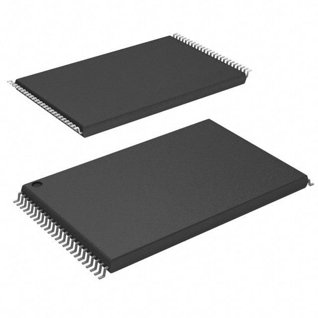
| Device Package | 48-TSOP I | Memory Format | FLASH | Technology | FLASH - NAND | ||
|---|---|---|---|---|---|---|---|
| Memory Size | 32 Gbit | Access Time | N/A | Grade | Commercial | ||
| Clock Frequency | N/A | Voltage | 2.7V ~ 3.6V | Memory Type | Non-Volatile | ||
| Operating Temperature | 0°C ~ 70°C (TA) | Write Cycle Time Word Page | N/A | Packaging | 48-TFSOP (0.724", 18.40mm Width) | ||
| Mounting Method | Non-Volatile | Memory Interface | Parallel | Memory Organization | 4G x 8 | ||
| Moisture Sensitivity Level | 3 (168 Hours) | RoHS Compliance | ROHS3 Compliant | REACH Compliance | REACH Unknown | ||
| Qualification | N/A | ECCN | 3A991B1A | HTS Code | 8542.32.0071 |
Overview of MT29F32G08AFABAWP:B TR – IC FLASH 32GBIT PAR 48TSOP I
The MT29F32G08AFABAWP:B TR is a 32 Gbit parallel NAND flash memory device in a 48‑TSOP I package. It implements NAND flash architecture with a 4G x 8 memory organization and supports both asynchronous and synchronous I/O modes.
Designed for embedded storage and data/code retention in systems operating at commercial temperatures, the device offers ONFI 2.2 compliance, multi-plane and cache commands, and voltage flexibility to support a range of host controllers and legacy parallel interfaces.
Key Features
- Core NAND Architecture 32 Gbit flash organized as 4G x 8 with page and block structures defined in the datasheet; supports single‑level cell technology as specified.
- Memory Organization & Capacity Page size (x8): 8,640 bytes (8,192 + 448), block size: 128 pages; device includes 4,096 blocks for the 32Gb density.
- Synchronous and Asynchronous Performance Synchronous I/O up to timing mode 5 with a 10 ns DDR clock (read/write throughput per pin up to 200 MT/s). Asynchronous I/O also supports up to timing mode 5 with per‑pin throughput up to 50 MT/s and RC/ WC = 20 ns (min).
- Interface & Command Support ONFI 2.2‑compliant parallel interface with data strobe (DQS) for synchronous operation. Advanced commands include program cache, read cache (sequential and random), multi‑plane commands, multi‑LUN operations, copyback, OTP mode, and read unique ID.
- Power Supply Options VCC operating range 2.7–3.6 V; VCCQ supported at 1.7–1.95 V or 2.7–3.6 V to accommodate host interface requirements.
- Reliability & Lifecycle Endurance specified at 80,000 program/erase cycles; data retention compliant with JESD47G (see qualification report for details). First block (block address 00h) is valid from factory.
- Package & Temperature 48‑TSOP I (0.724" / 18.40 mm width) package; commercial operating temperature range 0 °C to +70 °C.
- Startup & Status RESET (FFh) required as the first command after power‑on. Operation status byte provides software methods for detecting operation completion, pass/fail conditions and write‑protect status.
Typical Applications
- Embedded storage for consumer devices — Use as non‑volatile program and data storage in consumer electronics where commercial temperature support and a parallel NAND interface are required.
- Firmware and file system storage — Onboard code and file storage for embedded systems that benefit from multi‑plane commands, cache programming and read cache features.
- Industrial equipment (commercial range) — Data and configuration storage in equipment operating within 0 °C to +70 °C that requires proven NAND endurance and data retention characteristics.
- Legacy parallel NAND controller systems — Replacement or design‑in for systems using parallel ONFI‑compliant NAND with synchronous/asynchronous modes and DQS support.
Unique Advantages
- Flexible I/O modes: Supports both synchronous (with DQS) and asynchronous operation plus ONFI 2.2 compliance for compatibility with a range of host controllers.
- High endurance: Specified 80,000 program/erase cycles gives predictable lifecycle planning for repeated write/erase workloads.
- Advanced command set: Program and read cache, multi‑plane and multi‑LUN operations, copyback and OTP mode provide design flexibility and performance optimization.
- Voltage configuration options: VCCQ support at either 1.7–1.95 V or 2.7–3.6 V enables interface compatibility with different system designs.
- Factory‑ready first block: First block (block address 00h) is valid when shipped, simplifying initial deployment and validation.
- Compact TSOP footprint: 48‑TSOP I package (18.40 mm width) suits space‑constrained board designs that require parallel NAND memory.
Why Choose IC FLASH 32GBIT PAR 48TSOP I?
The MT29F32G08AFABAWP:B TR provides a well‑specified 32 Gbit parallel NAND solution that balances density, performance and endurance for embedded storage applications. With synchronous and asynchronous operating modes, ONFI 2.2 support and an advanced command set, it integrates into designs that need configurable throughput and legacy parallel interfaces.
This device is suited to engineers and procurement teams building commercial‑temperature systems that require reliable non‑volatile storage with clear electrical and mechanical specifications (2.7–3.6 V supply, 48‑TSOP I package). Its documented endurance and data retention characteristics support long‑term deployment planning and product lifecycle management.
Request a quote or submit a sales inquiry for pricing, availability and lead‑time information for the MT29F32G08AFABAWP:B TR.