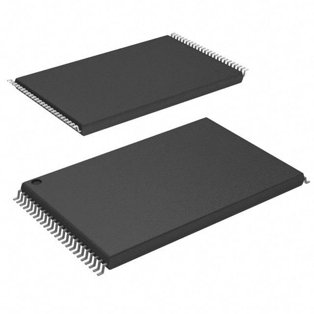
MT29F32G08AFABAWP:B
| Part Description |
IC FLASH 32GBIT PAR 48TSOP I |
|---|---|
| Quantity | 139 Available (as of June 15, 2026) |

| Product Category | Memory |
|---|---|
| Manufacturer | Micron Technology Inc. |
| Manufacturing Status | Obsolete |
| Manufacturer Standard Lead Time | Contact Us |
| Datasheet |
Specifications & Environmental
| Device Package | 48-TSOP I | Memory Format | FLASH | Technology | FLASH - NAND | ||
|---|---|---|---|---|---|---|---|
| Memory Size | 32 Gbit | Access Time | N/A | Grade | Commercial | ||
| Clock Frequency | N/A | Voltage | 2.7V ~ 3.6V | Memory Type | Non-Volatile | ||
| Operating Temperature | 0°C ~ 70°C (TA) | Write Cycle Time Word Page | N/A | Packaging | 48-TFSOP (0.724", 18.40mm Width) | ||
| Mounting Method | Non-Volatile | Memory Interface | Parallel | Memory Organization | 4G x 8 | ||
| Moisture Sensitivity Level | 3 (168 Hours) | RoHS Compliance | ROHS3 Compliant | REACH Compliance | REACH Unaffected | ||
| Qualification | N/A | ECCN | 3A991B1A | HTS Code | 8542.32.0071 |
Overview of MT29F32G08AFABAWP:B – IC FLASH 32GBIT PAR 48TSOP I
The MT29F32G08AFABAWP:B is a 32 Gbit parallel NAND flash memory device in a 48-pin TSOP I package. It implements NAND flash architecture with a 4G x 8 memory organization and supports both asynchronous and synchronous I/O modes.
Designed for systems that require non-volatile parallel storage, the device offers ONFI 2.2-compliant interface options, commercial temperature operation, and supply voltage flexibility suitable for a range of embedded applications.
Key Features
- Memory 32 Gbit (4G × 8) NAND flash memory with page and block organization specified for efficient block and page operations.
- Organization & Capacity Page size (×8): 8,640 bytes (8,192 + 448); Block size: 128 pages (1,024K + 56K bytes); Device configuration for 32Gb includes 4,096 blocks.
- Interface Parallel NAND interface supporting asynchronous and synchronous I/O; ONFI 2.2 compliant for standardized interface behavior.
- Performance Synchronous timing up to mode 5 with DDR clock rate (10 ns) and up to 200 MT/s per pin; asynchronous timing up to mode 5 with up to 50 MT/s per pin. Array timing examples: read page 35 μs (MAX), program page 350 μs (TYP), erase block 1.5 ms (TYP).
- Power Operating VCC range 2.7 V–3.6 V; VCCQ supported at 1.7–1.95 V or 2.7–3.6 V to accommodate different I/O voltage domains.
- Reliability Endurance rated at 80,000 program/erase cycles and data retention compliant with JESD47G as documented in the qualification report.
- Package & Temperature 48-pin TSOP I (48-TFSOP, 0.724", 18.40 mm width) package; commercial operating temperature range 0°C–70°C (TA).
- Advanced NAND Features Supports program cache, read cache (sequential and random), multi-plane and multi-LUN commands, copyback, read unique ID, and an OTP mode as described in the device specification.
Typical Applications
- Embedded Storage Use as parallel non-volatile storage where a 32 Gbit NAND footprint is required for system firmware, image storage, or bulk data retention.
- Consumer and Industrial Electronics Suitable for devices operating within the commercial temperature range that require standard TSOP packaging and parallel NAND interface.
- Data Logging and Boot Media Applicable for systems needing reliable program/erase endurance and standardized NAND command sets for boot code and log storage.
Unique Advantages
- High Density 32 Gbit Capacity: Delivers 4G × 8 organization for substantial non-volatile storage in a compact TSOP package.
- Flexible Interface Modes: Supports both asynchronous and synchronous I/O with ONFI 2.2 compatibility for easier integration with host controllers that use parallel NAND signaling.
- Performance-Tuned Array Operations: Documented read, program, and erase latencies (e.g., read page 35 μs, program page 350 μs) enable predictable system timing budgets.
- Robust Endurance: Rated for 80,000 program/erase cycles, offering longevity for applications with frequent write/erase activity.
- Voltage Flexibility: Wide VCC and VCCQ options (2.7 V–3.6 V and 1.7 V–1.95 V / 2.7 V–3.6 V) accommodate various system power domains.
- Standard TSOP Package: 48-TSOP I package provides a common footprint for board-level integration and thermal/mechanical familiarity.
Why Choose IC FLASH 32GBIT PAR 48TSOP I?
The MT29F32G08AFABAWP:B targets designs that require a 32 Gbit parallel NAND flash solution with documented performance, endurance, and a standard TSOP package. Its ONFI 2.2 compliance and support for synchronous and asynchronous modes make it suitable for systems that need predictable I/O timing and standardized command behavior.
This device is appropriate for engineers specifying non-volatile storage where density, endurance, and interface flexibility are primary selection criteria. The combination of capacity, array timing data, and package options supports scalable designs and straightforward board-level integration.
Request a quote or submit a sales inquiry for pricing, availability, and lead-time information for MT29F32G08AFABAWP:B.