MT29F32G08AECCBH1-10Z:C
| Part Description |
IC FLASH 32GBIT PARALLEL 100VBGA |
|---|---|
| Quantity | 1,852 Available (as of June 15, 2026) |

| Product Category | Memory |
|---|---|
| Manufacturer | Micron Technology Inc. |
| Manufacturing Status | Obsolete |
| Manufacturer Standard Lead Time | Contact Us |
| Datasheet |
Specifications & Environmental
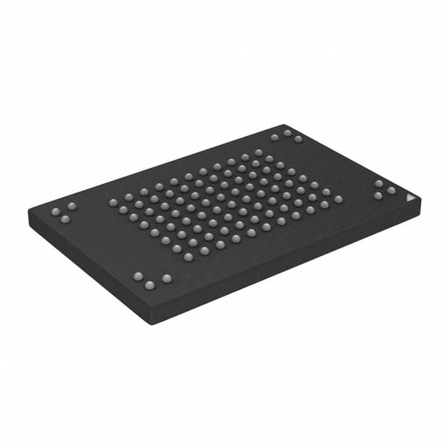
| Device Package | 100-VBGA (12x18) | Memory Format | FLASH | Technology | FLASH - NAND | ||
|---|---|---|---|---|---|---|---|
| Memory Size | 32 Gbit | Access Time | N/A | Grade | Commercial | ||
| Clock Frequency | 100 MHz | Voltage | 2.7V ~ 3.6V | Memory Type | Non-Volatile | ||
| Operating Temperature | 0°C ~ 70°C (TA) | Write Cycle Time Word Page | N/A | Packaging | 100-VBGA | ||
| Mounting Method | Non-Volatile | Memory Interface | Parallel | Memory Organization | 4G x 8 | ||
| Moisture Sensitivity Level | 3 (168 Hours) | RoHS Compliance | ROHS Compliant | REACH Compliance | REACH Unaffected | ||
| Qualification | N/A | ECCN | 3A991B1A | HTS Code | 8542.32.0071 |
Overview of MT29F32G08AECCBH1-10Z:C – 32Gbit Parallel NAND Flash (100‑VBGA)
The MT29F32G08AECCBH1-10Z:C is a 32 Gbit non-volatile NAND flash memory device in a 100-ball VBGA (12×18) package. It uses NAND flash architecture with a parallel interface and is supplied for operation from 2.7 V to 3.6 V, providing on-board storage for embedded systems and other applications that require persistent data storage.
Designed with synchronous and asynchronous I/O modes and ONFI 2.2-compliant features, the device targets applications that need deterministic read/write behavior, data retention visibility and established NAND command support.
Key Features
- Memory Architecture 32 Gbit capacity organized as 4G × 8 with device-level structure documented for 32Gb density (4096 blocks per device); page and block geometry specified in the product family datasheet.
- Interface and Timing Parallel memory interface with a listed clock frequency of 100 MHz; supports both synchronous and asynchronous I/O modes per the device family.
- ONFI and Data Strobe ONFI 2.2-compliant features and DQS (data strobe) support for hardware synchronization of DQ in synchronous mode.
- Performance Characteristics Documented array timings include read page ≤ 35 μs (max), program page ≈ 350 μs (typ), and erase block ≈ 1.5 ms (typ); synchronous and asynchronous throughput metrics are provided in the datasheet for performance planning.
- Advanced Command Set Supports program cache, read cache (sequential and random), multi-plane commands, multi-LUN operations, copyback, OTP mode and read unique ID as described in the product documentation.
- Power and Voltage VCC operating range 2.7 V–3.6 V; VCCQ supported at 1.7–1.95 V or 2.7–3.6 V depending on interface configuration.
- Endurance and Reliability Endurance rated at 80,000 program/erase cycles with data retention and qualification references provided in the datasheet (JESD47G compliance noted for retention).
- Package and Thermal 100-ball BGA package (100‑VBGA, 12×18) with commercial operating temperature range 0 °C to +70 °C.
- Power-On and Status RESET (FFh) required as the first command after power-on and device provides an operation status byte for completion, pass/fail and write-protect indicators.
Typical Applications
- Embedded Storage Non-volatile storage for embedded systems requiring NAND flash for firmware, file storage or data logging.
- Boot and Firmware Storage Persistent device memory for storing boot code and system firmware where documented ECC and block management are applied.
- Data Logging and Retention Field data capture and retention applications that benefit from the device's endurance and documented data retention qualifications.
Unique Advantages
- Documented ONFI Compliance: ONFI 2.2 feature set and DQS support simplify integration with controllers that implement the ONFI protocol.
- High Endurance: Endurance rating of 80,000 program/erase cycles supports long life in write-intensive embedded use cases.
- Flexible Voltage Options: Broad VCC range (2.7–3.6 V) and VCCQ options enable compatibility with differing system supplies and interface requirements.
- Compact, Standard Package: 100-ball VBGA (12×18) package provides a compact footprint for space-constrained PCB designs.
- Comprehensive Command Set: Advanced features such as program/read caches, multi-plane and multi-LUN operations allow optimized throughput and maintenance strategies.
- Measured Array Performance: Published read/program/erase timing figures in the datasheet help designers budget latency and throughput in system design.
Why Choose IC FLASH 32GBIT PARALLEL 100VBGA?
The MT29F32G08AECCBH1-10Z:C provides a documented NAND flash solution with 32 Gbit capacity, robust endurance and ONFI 2.2 feature support in a compact 100‑VBGA package. Its combination of synchronous/asynchronous modes, DQS support, and an advanced command set makes it suitable for embedded applications that require deterministic NAND behavior and lifetime predictability.
This device is well suited to designs where verified endurance, published timing characteristics and flexible voltage operation are required. The datasheet supplies the technical details needed for integration, ECC planning and system-level performance estimation.
Request a quote or submit a sourcing inquiry to receive pricing and availability information for the MT29F32G08AECCBH1-10Z:C.