MT29F32G08AFACAWP-Z:C
| Part Description |
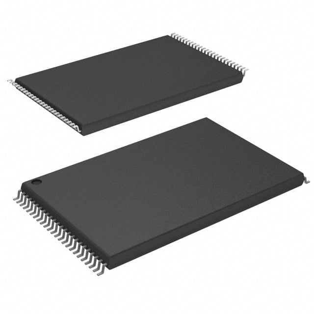
IC FLASH 32GBIT PAR 48TSOP I |
|---|---|
| Quantity | 1,097 Available (as of June 15, 2026) |

| Product Category | Memory |
|---|---|
| Manufacturer | Micron Technology Inc. |
| Manufacturing Status | Obsolete |
| Manufacturer Standard Lead Time | Contact Us |
| Datasheet |
Specifications & Environmental
| Device Package | 48-TSOP I | Memory Format | FLASH | Technology | FLASH - NAND | ||
|---|---|---|---|---|---|---|---|
| Memory Size | 32 Gbit | Access Time | N/A | Grade | Commercial | ||
| Clock Frequency | N/A | Voltage | 2.7V ~ 3.6V | Memory Type | Non-Volatile | ||
| Operating Temperature | 0°C ~ 70°C (TA) | Write Cycle Time Word Page | N/A | Packaging | 48-TFSOP (0.724", 18.40mm Width) | ||
| Mounting Method | Non-Volatile | Memory Interface | Parallel | Memory Organization | 4G x 8 | ||
| Moisture Sensitivity Level | 3 (168 Hours) | RoHS Compliance | ROHS3 Compliant | REACH Compliance | REACH Unaffected | ||
| Qualification | N/A | ECCN | 3A991B1A | HTS Code | 8542.32.0071 |
Overview of MT29F32G08AFACAWP-Z:C – IC FLASH 32GBIT PAR 48TSOP I
The MT29F32G08AFACAWP-Z:C is a 32 Gbit NAND flash memory device using NAND flash technology with a parallel interface and 4G x 8 organization. It implements asynchronous and synchronous NAND operation and is offered in a 48-TSOP I package suitable for commercial-temperature applications.
Designed for non-volatile storage in systems requiring ONFI-compliant NAND functionality, the device provides advanced command features and a range of interface timing modes to support varied controller implementations.
Key Features
- Core / Memory Architecture 32 Gbit NAND flash organized as 4G × 8 with single-level cell (SLC) technology; the 32Gb device contains 4,096 blocks.
- Page and Block Organization Page size x8 is 8,640 bytes (8,192 + 448); block size is 128 pages (1,024K + 56K bytes); two planes with 2,048 blocks per plane are provided.
- Interface & Standards Parallel NAND interface with ONFI 2.2 compliance; supports both asynchronous and synchronous I/O modes and up to synchronous timing mode 5.
- Performance Synchronous read/write throughput up to 200 MT/s per pin; asynchronous throughput up to 50 MT/s per pin; DDR-capable clock rate noted at 10 ns.
- Typical Latencies Read page: 35 μs (MAX); Program page: 350 μs (TYP); Erase block: 1.5 ms (TYP).
- Advanced Command Set Supports program cache, read cache (sequential and random), one-time programmable (OTP) mode, multi-plane commands, multi-LUN operations, copyback and read unique ID.
- Power Operating VCC: 2.7–3.6 V. VCCQ options documented at 1.7–1.95 V or 2.7–3.6 V.
- Reliability & Endurance Endurance rated at 80,000 program/erase cycles with data retention compliant to JESD47G as stated in the device documentation.
- Package & Temperature Available in a 48-TFSOP (48-TSOP I) package — 0.724" (18.40 mm) width — and specified for commercial operating temperature: 0 °C to +70 °C (TA).
Unique Advantages
- Flexible Timing Modes: Support for both asynchronous and synchronous operation (including DDR timing) provides design flexibility across controller implementations.
- ONFI 2.2 Compatibility: Conformance to the ONFI 2.2 specification enables interoperability with ONFI-aware host controllers.
- SLC Endurance: Single-level cell architecture with 80,000 program/erase cycles supports extended device lifetime for write-intensive applications.
- Comprehensive Command Feature Set: Program/read caching, multi-plane and multi-LUN commands, OTP and copyback simplify advanced memory management and controller integration.
- Standard TSOP Package: 48-TSOP I package (18.40 mm width) provides a common board-level footprint for integration into commercial designs.
- Broad Supply Options: VCC and VCCQ ranges accommodate typical NAND power schemes (2.7–3.6 V with documented VCCQ options).
Why Choose MT29F32G08AFACAWP-Z:C?
The MT29F32G08AFACAWP-Z:C positions itself as a commercial-temperature, parallel-interface NAND flash solution that combines SLC endurance, ONFI 2.2 protocol support, and a comprehensive command set for advanced NAND operations. Its documented latencies, throughput ranges for synchronous and asynchronous modes, and package options make it suitable for designers specifying non-volatile NAND memory with predictable performance and integration characteristics.
This device is appropriate for designs requiring a 32 Gbit NAND flash with robust program/erase endurance and standard TSOP packaging from a known NAND memory manufacturer. The device documentation provides the electrical, timing and command details needed for controller integration and system validation.
Request a quote or submit a sales inquiry to evaluate MT29F32G08AFACAWP-Z:C for your next design requirement.