MT46V128M4TG-6T:F TR
| Part Description |
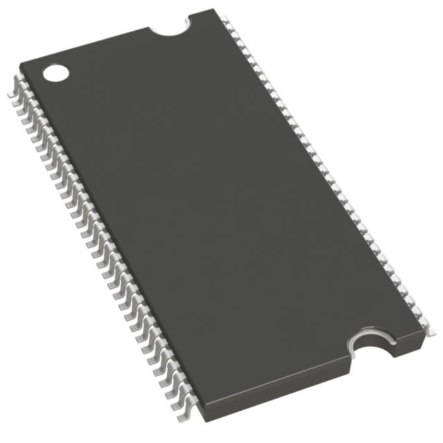
IC DRAM 512MBIT PAR 66TSOP |
|---|---|
| Quantity | 773 Available (as of June 17, 2026) |
| Product Category | DRAM Memory |
|---|---|
| Manufacturer | Micron Technology Inc. |
| Manufacturing Status | Obsolete |
| Manufacturer Standard Lead Time | Contact Us |
| Datasheet |
Specifications & Environmental
| Device Package | 66-TSOP | Memory Format | DRAM | Technology | SDRAM - DDR | ||
|---|---|---|---|---|---|---|---|
| Memory Size | 512 Mbit | Access Time | 700 ps | Grade | Commercial | ||
| Clock Frequency | 167 MHz | Voltage | 2.3V ~ 2.7V | Memory Type | Volatile | ||
| Operating Temperature | 0°C ~ 70°C (TA) | Write Cycle Time Word Page | 15 ns | Packaging | 66-TSSOP (0.400", 10.16mm Width) | ||
| Mounting Method | Volatile | Memory Interface | Parallel | Memory Organization | 128M x 4 | ||
| Moisture Sensitivity Level | 4 (72 Hours) | RoHS Compliance | RoHS non-compliant | REACH Compliance | REACH Unaffected | ||
| Qualification | N/A | ECCN | EAR99 | HTS Code | 8542.32.0024 |
Overview of MT46V128M4TG-6T:F TR – IC DRAM 512MBIT PAR 66TSOP
The MT46V128M4TG-6T:F TR is a 512 Mbit DDR SDRAM device organized as 128M × 4 with a parallel memory interface in a 66‑TSSOP package. It implements an internal pipelined double-data-rate architecture with four internal banks and source‑synchronous data capture for high-efficiency memory transfers.
Designed for commercial-temperature systems, this device delivers defined timing at a 167 MHz clock frequency, 2.3–2.7 V supply range, and package options that suit board-level integration where a 128M × 4 DDR memory is required.
Key Features
- Core / Memory Architecture 512 Mbit DDR SDRAM organized as 128M × 4 with four internal banks and an internal pipelined DDR architecture (two data accesses per clock cycle).
- Performance & Timing Speed grade 6T supports a 167 MHz clock frequency with an access time as low as 700 ps and timing characteristics defined for CL = 2.5 in the datasheet.
- Data Strobe & Alignment Bidirectional data strobe (DQS) is transmitted/received with data for source‑synchronous capture; DQS is edge‑aligned for READs and center‑aligned for WRITEs, and a DLL aligns DQ/DQS transitions with CK.
- Interface & Commands Differential clock inputs (CK and CK#) with commands entered on each positive CK edge; data mask (DM) supported for write masking.
- Burst and Refresh Programmable burst lengths of 2, 4, or 8; supports auto refresh with 8K refresh cycles (64 ms interval for commercial devices) and self refresh options as noted in the datasheet.
- Power & I/O Operates from 2.3 V to 2.7 V supply; 2.5 V I/O (SSTL_2 compatible) per datasheet specifications.
- Package & Temperature 66‑TSSOP (0.400", 10.16 mm width) plastic package; commercial operating temperature range 0°C to +70°C (TA).
- Additional Reliability Features Four internal banks for concurrent operation and longer‑lead TSOP option noted for improved reliability (OCPL) in the product documentation.
Typical Applications
- Memory expansion for embedded systems Provides 512 Mbit of parallel DDR SDRAM capacity (128M × 4 organization) for designs requiring defined timing and source‑synchronous DQS.
- Board-level DDR implementations Suited for systems using differential CK/CK# inputs, DLL alignment, and programmable burst lengths to manage high‑speed transfers.
- Commercial-grade electronics Used in designs that operate across a 0°C to 70°C ambient range and require 2.5 V I/O signaling compatibility.
Unique Advantages
- Deterministic timing at 167 MHz Speed grade 6T timing parameters and defined data‑out/access windows enable repeatable timing budgets for system designers.
- Source-synchronous data capture Bidirectional DQS combined with a DLL and DQ/DQS alignment reduces timing uncertainty for reads and writes.
- Flexible burst control Programmable burst lengths (2, 4, 8) let designers balance latency and throughput per application needs.
- Robust refresh management Auto refresh with 8K cycle refresh and self‑refresh options provide standard DRAM refresh strategies documented in the datasheet.
- Board-friendly package 66‑TSSOP (10.16 mm width) package provides a compact, longer‑lead TSOP option referenced for improved reliability in the documentation.
- Standard SSTL_2 I/O levels 2.5 V I/O compatibility supports designs that require standard DDR I/O signaling levels.
Why Choose MT46V128M4TG-6T:F TR?
The MT46V128M4TG-6T:F TR positions itself as a straightforward 512 Mbit DDR SDRAM solution for commercial‑temperature designs that need a 128M × 4 organization, defined 6T timing at 167 MHz, and standard 66‑TSSOP packaging. Its source‑synchronous DQS, DLL alignment, programmable burst lengths, and documented refresh behavior support reliable, repeatable memory operation.
This device is suited to system designers and procurement teams specifying board‑level DDR memory where compatibility with 2.5 V I/O, a 2.3–2.7 V supply window, and a commercial operating range are required. The datasheet provides the detailed timing, refresh, and package information needed for integration and validation in such designs.
Request a quote or submit an inquiry to receive pricing and availability information for the MT46V128M4TG-6T:F TR.