MT46V16M16CY-5B AAT:M TR
| Part Description |
IC DRAM 256MBIT PARALLEL 60FBGA |
|---|---|
| Quantity | 820 Available (as of June 14, 2026) |

| Product Category | Memory |
|---|---|
| Manufacturer | Micron Technology Inc. |
| Manufacturing Status | Obsolete |
| Manufacturer Standard Lead Time | Contact Us |
| Datasheet |
Specifications & Environmental
| Device Package | 60-FBGA (8x12.5) | Memory Format | DRAM | Technology | SDRAM - DDR | ||
|---|---|---|---|---|---|---|---|
| Memory Size | 256 Mbit | Access Time | 700 ps | Grade | Automotive | ||
| Clock Frequency | 200 MHz | Voltage | 2.5V ~ 2.7V | Memory Type | Volatile | ||
| Operating Temperature | -40°C ~ 105°C (TA) | Write Cycle Time Word Page | 15 ns | Packaging | 60-TFBGA | ||
| Mounting Method | Volatile | Memory Interface | Parallel | Memory Organization | 16M x 16 | ||
| Moisture Sensitivity Level | 3 (168 Hours) | RoHS Compliance | ROHS3 Compliant | REACH Compliance | REACH Unaffected | ||
| Qualification | AEC-Q100 | ECCN | EAR99 | HTS Code | 8542.32.0036 |
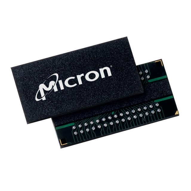
Overview of MT46V16M16CY-5B AAT:M TR – IC DRAM 256MBIT PARALLEL 60FBGA
The MT46V16M16CY-5B AAT:M TR is a 256 Mbit DDR SDRAM device organized as 16M × 16 with a parallel memory interface in a 60-ball TFBGA (8 mm × 12.5 mm) package. It implements an internal, pipelined double-data-rate architecture with source-synchronous DQS and differential clock inputs for two data transfers per clock cycle.
Targeted for applications requiring automotive-grade memory, this AAT-marked device is AEC‑Q100 qualified and specified for operation from −40°C to +105°C, supporting VDD/VDDQ nominally in the 2.5 V–2.7 V range and timing up to 200 MHz (−5B timing grade).
Key Features
- Core / Architecture Internal pipelined DDR architecture providing two data accesses per clock cycle, four internal banks, DLL for DQ/DQS alignment, and differential clock inputs (CK/CK#); commands are entered on each positive CK edge.
- Memory Organization 256 Mbit capacity organized as 16M × 16 with two DQS lines (one per byte) and two data mask (DM) signals for byte masking on writes.
- Timing & Performance −5B timing grade supports up to 200 MHz clock rate (CL = 3); datasheet timing examples include data-out and access windows and a DQS–DQ skew specification for reliable source-synchronous capture.
- Read/Write and Burst Programmable burst lengths of 2, 4, or 8 with DQS edge alignment center-aligned for writes and edge-aligned for reads; write-cycle time (word/page) specified at 15 ns.
- Power / Voltage Supply range specified at 2.5 V–2.7 V; datasheet notes VDD/VDDQ nominal scenarios for standard and DDR400 operating conditions.
- Reliability & Automotive Qualification AEC‑Q100 qualified with AAT temperature rating (−40°C to +105°C); PPAP submission and 8D response are documented in the datasheet. Note: self refresh is not available on AAT devices.
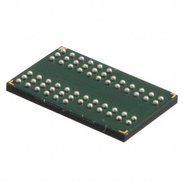
- Package & Mounting 60-ball TFBGA package (8 mm × 12.5 mm) intended for surface-mount assembly in space-constrained system boards.
Typical Applications
- Automotive electronics — DDR memory for automotive systems that require AEC‑Q100 qualification and −40°C to +105°C operation.
- Embedded systems — volatile DDR storage for embedded controllers and processors needing a 256 Mbit parallel DDR interface.
- High-speed buffering — source-synchronous DQS and differential clocking make the device suitable for buffering and temporary data storage in systems using parallel DDR memory.
Unique Advantages
- Automotive-grade qualification: AEC‑Q100 rating and AAT temperature range support use in automotive electronics that require elevated temperature operation.
- Source-synchronous data capture: Bidirectional DQS with DLL alignment enables reliable read/write timing and byte-level data strobes for accurate sampling.
- Compact FBGA package: 60-ball TFBGA (8 mm × 12.5 mm) provides a small footprint for board designs with limited space.
- Flexible burst and bank architecture: Programmable burst lengths (2/4/8) and four internal banks permit concurrent operations and adaptable access patterns.
- Defined supply and timing envelopes: Specified supply range (2.5 V–2.7 V), access timing (700 ps listed access window), and −5B timing grade support predictable electrical integration.
Why Choose IC DRAM 256MBIT PARALLEL 60FBGA?
The MT46V16M16CY-5B AAT:M TR provides a purpose-built 256 Mbit DDR SDRAM option for designs that require a parallel DDR interface with automotive-grade validation. Its pipelined DDR architecture, source-synchronous DQS, and four-bank organization deliver deterministic, double-data-rate transfers suitable for systems demanding controlled timing and temperature resilience.
This device is appropriate for engineers specifying memory for automotive and embedded applications that need a compact FBGA package, defined timing grades (−5B up to 200 MHz), and AEC‑Q100 qualification. Its documented timing and supply parameters support straightforward integration into DDR memory subsystems where reliable, verifiable specifications are required.
Request a quote or contact sales to discuss availability, lead times, and pricing for MT46V16M16CY-5B AAT:M TR.