MT46V32M16BN-5B IT:F
| Part Description |
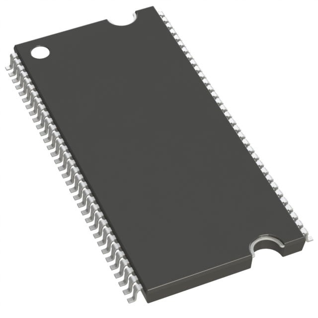
IC DRAM 512MBIT PARALLEL 60FBGA |
|---|---|
| Quantity | 1,158 Available (as of June 13, 2026) |

| Product Category | Memory |
|---|---|
| Manufacturer | Micron Technology Inc. |
| Manufacturing Status | Obsolete |
| Manufacturer Standard Lead Time | Contact Us |
| Datasheet |
Specifications & Environmental
| Device Package | 60-FBGA (10x12.5) | Memory Format | DRAM | Technology | SDRAM - DDR | ||
|---|---|---|---|---|---|---|---|
| Memory Size | 512 Mbit | Access Time | 700 ps | Grade | Industrial | ||
| Clock Frequency | 200 MHz | Voltage | 2.5V ~ 2.7V | Memory Type | Volatile | ||
| Operating Temperature | -40°C ~ 85°C (TA) | Write Cycle Time Word Page | 15 ns | Packaging | 60-TFBGA | ||
| Mounting Method | Volatile | Memory Interface | Parallel | Memory Organization | 32M x 16 | ||
| Moisture Sensitivity Level | 3 (168 Hours) | RoHS Compliance | ROHS3 Compliant | REACH Compliance | REACH Unaffected | ||
| Qualification | N/A | ECCN | EAR99 | HTS Code | 8542.32.0028 |
Overview of MT46V32M16BN-5B IT:F – IC DRAM 512MBIT PARALLEL 60FBGA
The MT46V32M16BN-5B IT:F is a 512 Mbit DDR SDRAM device organized as 32M × 16 with a parallel memory interface in a 60-ball FBGA package. It implements a Double Data Rate (DDR) architecture with internal DLL, differential clock inputs and source‑synchronous DQS for high‑speed data transfer.
This device targets designs that require compact, industrial‑temperature DDR memory for temporary data storage and high‑throughput buffering, offering specified clock performance, programmable burst lengths and standard 2.5 V I/O levels.
Key Features
- Core / Architecture Double Data Rate (DDR) SDRAM with internal pipelined DDR architecture and a DLL to align DQ/DQS transitions with CK; supports two data accesses per clock cycle.
- Memory Organization & Capacity 512 Mbit device organized as 32M × 16 with four internal banks (8 Meg × 16 × 4 banks configuration).
- Speed & Timing -5B speed grade: 5 ns cycle time (CL = 3) supporting up to 200 MHz clock rate; access window and timing details per datasheet (data-out window and DQS‑DQ skew specified).
- Data I/O and Strobes Bidirectional data strobe (DQS) transmitted/received with data; x16 devices include two DQS and two data masks (DM) — one per byte.
- Clock & Command Differential clock inputs (CK and CK#) with commands entered on positive CK edge and DQS edge‑alignment center for writes and edge‑aligned for reads.
- Power Standard VDD/VDDQ = +2.5 V ±0.2 V; DDR400 option supports VDD/VDDQ = +2.6 V ±0.1 V.
- Refresh & Burst Auto refresh with 8192‑cycle / 64 ms refresh interval and programmable burst lengths of 2, 4, or 8.
- Package 60‑ball FBGA package (10 mm × 12.5 mm) in a compact footprint suitable for board‑level integration.
- Industrial Temperature Range Specified operating temperature from −40°C to +85°C (TA) for industrial applications.
- Write and Access Characteristics Write cycle time (word/page) specified at 15 ns and an access time listed as 700 ps in product specifications.
Typical Applications
- Industrial systems Memory subsystem for industrial equipment that requires DDR SDRAM operating across −40°C to +85°C.
- Compact board‑level memory 60‑ball FBGA (10 mm × 12.5 mm) package for space‑constrained designs needing on‑board DRAM.
- High‑throughput buffering Temporary data storage and buffering in systems that leverage DDR source‑synchronous DQS and programmable burst lengths for burst transfers.
Unique Advantages
- Double data‑rate transfers: Enables two data accesses per clock cycle via DDR architecture, improving effective throughput without changing clock frequency.
- Industrial temperature rating: −40°C to +85°C operating range supports deployment in industrial environments where extended temperature tolerance is required.
- Standard 2.5 V I/O (SSTL_2 compatible): VDD/VDDQ specifications of +2.5 V ±0.2 V provide compatibility with standard 2.5 V signaling domains.
- Compact FBGA package: 60‑ball FBGA (10 mm × 12.5 mm) offers a small footprint for dense PCBs and board‑level memory integration.
- Flexible timing and refresh: Programmable burst lengths, auto refresh (8192 cycles / 64 ms) and defined speed grades (e.g., -5B) allow designers to balance latency and throughput.
- Byte‑level control: Data mask (DM) and dual DQS on x16 enable byte‑level write masking and robust source‑synchronous data capture.
Why Choose MT46V32M16BN-5B IT:F?
The MT46V32M16BN-5B IT:F delivers a verified 512 Mbit DDR SDRAM solution with industry‑grade temperature range, defined timing grades and compact FBGA packaging. Its DDR architecture, differential clocking and DQS‑based source‑synchronous capture provide deterministic timing behavior required for high‑speed parallel memory designs.
This device is suited to designs that need a reliable, board‑level DDR memory component with clear electrical and timing specifications (VDD/VDDQ, clock rates, access/write timings) and industrial temperature capability. Detailed datasheet timing and configuration information support predictable integration and long‑term deployment in industrial and compact system designs.
Request a quote or submit a sales inquiry for MT46V32M16BN-5B IT:F with your required quantity and lead‑time details to receive pricing and availability information.